- 您現在的位置:買賣IC網 > PDF目錄373961 > AD9241 (Analog Devices, Inc.) Complete 14-Bit, 1.25 MSPS Monolithic A/D Converter PDF資料下載
參數資料
| 型號: | AD9241 |
| 廠商: | Analog Devices, Inc. |
| 英文描述: | Complete 14-Bit, 1.25 MSPS Monolithic A/D Converter |
| 中文描述: | 完整的14位,125 MSPS的單片機的A / D轉換器 |
| 文件頁數: | 16/24頁 |
| 文件大小: | 495K |
| 代理商: | AD9241 |
AD9241
REV. 0
–16–
Shorting the VREF pin directly to the SENSE pin places the
internal reference amplifier in unity-gain mode and the resultant
VREF output is 1 V. Therefore, the valid input range is 0 V to
2 V. However, shorting the SENSE pin directly to the REFCOM
pin configures the internal reference amplifier for a gain of 2.5
and the resultant VREF output is 2.5 V. Thus, the valid input
range becomes 0 V to 5 V. The VREF pin should be bypassed
to the REFCOM pin with a 10
μ
F tantalum capacitor in parallel
with a low-inductance 0.1
μ
F ceramic capacitor.
10μF
VINA
VREF
AD9241
0.1μF
VINB
2xVREF
0V
SHORT FOR 0 TO 2V
INPUT SPAN
SENSE
SHORT FOR 0 TO 5V
INPUT SPAN
REFCOM
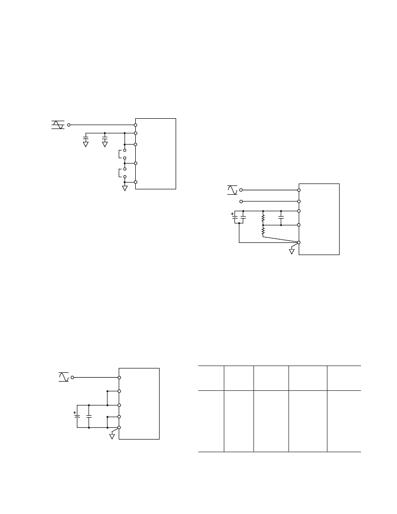
Figure 36. Internal Reference (2 V p-p Input Span,
V
CM
= 1 V, or 5 V p-p Input Span, V
CM
= 2.5 V)
Single-Ended or Differential Input, V
CM
= 2.5 V
Figure 37 shows the single-ended configuration that gives the
best SINAD performance. To optimize dynamic specifications,
center the common-mode voltage of the analog input at
approximately 2.5 V by connecting VINB to VREF, a low-
impedance 2.5 V source. As described above, shorting the
SENSE pin directly to the REFCOM pin results in a 2.5 V
reference voltage and a 5 V p-p input span. The valid range
for input signals is 0 V to 5 V. The VREF pin should be by-
passed to the REFCOM pin with a 10
μ
F tantalum capacitor in
parallel with a low inductance 0.1
μ
F ceramic capacitor.
This reference configuration could also be used for a differential
input wherein VINA and VINB are driven via a transformer as
shown in Figure 29. In this case, the common-mode voltage,
V
CM
, is set at midsupply by connecting the transformers center
tap to CML of the AD9241. VREF can be configured for 1 V or
2.5 V by connecting SENSE to either VREF or REFCOM
respectively. Note that the valid input range for each of the
differential inputs is one half of the single-ended input and thus
becomes V
CM
– VREF/2 to V
CM
+ VREF/2.
0.1μF
10μF
VINA
VINB
VREF
SENSE
REFCOM
AD9241
5V
0V
2.5V
Figure 37. Internal Reference—5 V p-p Input Span,
V
CM
= 2.5 V
Resistor Programmable Reference
Figure 38 shows an example of how to generate a reference
voltage other than 1 V or 2.5 V with the addition of two ex-
ternal resistors and a bypass capacitor. Use the equation,
VREF
= 1
V
×
(1 +
R
1/
R
2),
to determine appropriate values for
R
1 and
R
2. These resistors
should be in the 2 k
to 100 k
range. For the example shown,
R
1 equals 2.5 k
and
R
2 equals 5 k
. From the equation above,
the resultant reference voltage on the VREF pin is 1.5 V. This
sets the input span to be 3 V p-p. To assure stability, place a
0.1
μ
F ceramic capacitor in parallel with
R
1.
The common-mode voltage can be set to VREF by connecting
VINB to VREF to provide an input span of 0 to 2
×
VREF.
Alternatively, the common-mode voltage can be set to 2.5 V
by connecting VINB to a low impedance 2.5 V source. For
the example shown, the valid input signal range for VINA is
1 V to 4 V since VINB is set to an external, low impedance
2.5 V source. The VREF pin should be bypassed to the REFCOM
pin with a 10
μ
F tantalum capacitor in parallel with a low induc-
tance 0.1
μ
F ceramic capacitor.
1.5V
C1
0.1μF
10μF
VINA
VINB
VREF
SENSE
REFCOM
AD9241
4V
1V
2.5V
R1
2.5k
R2
5k
0.1μF
Figure 38. Resistor Programmable Reference (3 V p-p
Input Span, V
CM
= 2.5 V)
USING AN EXTERNAL REFERENCE
Using an external reference may enhance the dc performance
of the AD9241 by improving drift and accuracy. Figures 39
through 41 show examples of how to use an external reference
with the A/D. Table III is a list of suitable voltage references
from Analog Devices. To use an external reference, the user
must disable the internal reference amplifier and drive the VREF
pin. Connecting the SENSE pin to AVDD disables the inter-
nal reference amplifier.
Table III. Suitable Voltage References
Initial
Accuracy
% (max)
Operating
Current
(
m
A)
Output
Voltage
Drift
(ppm/
8
C)
Internal
AD589
AD1580
REF191
Internal
REF192
REF43
AD780
1.00
1.235
1.225
2.048
2.50
2.50
2.50
2.50
26
10–100
50–100
5–25
26
5–25
10–25
3–7
1.4
1.2–2.8
0.08–0.8
0.1–0.5
1.4
0.08–0.4
0.06–0.1
0.04–0.2
N/A
50
50
45
N/A
45
600
1000
The AD9241 contains an internal reference buffer, A2 (see
Figure 26), that simplifies the drive requirements of an external
reference. The external reference must be able to drive a
≈
5 k
(
±
20%) load. Note that the bandwidth of the reference buffer is
相關PDF資料 |
PDF描述 |
|---|---|
| AD9241AS | RES., MF, 2K, 1%, 1/4W |
| AD9241EB | Complete 14-Bit, 1.25 MSPS Monolithic A/D Converter |
| AD9243 | Complete 14-Bit, 3.0 MSPS Monolithic A/D Converter |
| AD9243AS | Complete 14-Bit, 3.0 MSPS Monolithic A/D Converter |
| AD9243EB | Complete 14-Bit, 3.0 MSPS Monolithic A/D Converter |
相關代理商/技術參數 |
參數描述 |
|---|---|
| AD9241ACHIPS | 制造商:Analog Devices 功能描述: |
| AD9241AS | 制造商:Analog Devices 功能描述:ADC Single Pipelined 1.25Msps 14-bit Parallel 44-Pin MQFP 制造商:Rochester Electronics LLC 功能描述:14BIT 1.25 MSPS MONOLITHIC A/D CONVERTER - Bulk 制造商:Analog Devices 功能描述:IC 14-BIT ADC |
| AD9241ASRL | 制造商:Analog Devices 功能描述:ADC Single Pipelined 1.25Msps 14-bit Parallel 44-Pin MQFP T/R |
| AD9241ASZ | 功能描述:IC ADC 14BIT 1.25MSPS 44-MQFP RoHS:是 類別:集成電路 (IC) >> 數據采集 - 模數轉換器 系列:- 標準包裝:1 系列:microPOWER™ 位數:8 采樣率(每秒):1M 數據接口:串行,SPI? 轉換器數目:1 功率耗散(最大):- 電壓電源:模擬和數字 工作溫度:-40°C ~ 125°C 安裝類型:表面貼裝 封裝/外殼:24-VFQFN 裸露焊盤 供應商設備封裝:24-VQFN 裸露焊盤(4x4) 包裝:Digi-Reel® 輸入數目和類型:8 個單端,單極 產品目錄頁面:892 (CN2011-ZH PDF) 其它名稱:296-25851-6 |
| AD9241ASZRL | 功能描述:IC ADC 14BIT SGL 1.25MSPS 44MQFP RoHS:是 類別:集成電路 (IC) >> 數據采集 - 模數轉換器 系列:- 標準包裝:1,000 系列:- 位數:12 采樣率(每秒):300k 數據接口:并聯 轉換器數目:1 功率耗散(最大):75mW 電壓電源:單電源 工作溫度:0°C ~ 70°C 安裝類型:表面貼裝 封裝/外殼:24-SOIC(0.295",7.50mm 寬) 供應商設備封裝:24-SOIC 包裝:帶卷 (TR) 輸入數目和類型:1 個單端,單極;1 個單端,雙極 |
發布緊急采購,3分鐘左右您將得到回復。