- 您現在的位置:買賣IC網 > PDF目錄373963 > AD9432BST-80 (ANALOG DEVICES INC) 12-Bit, 80 MSPS/105 MSPS A/D Converter PDF資料下載
參數資料
| 型號: | AD9432BST-80 |
| 廠商: | ANALOG DEVICES INC |
| 元件分類: | ADC |
| 英文描述: | 12-Bit, 80 MSPS/105 MSPS A/D Converter |
| 中文描述: | 1-CH 12-BIT PROPRIETARY METHOD ADC, PARALLEL ACCESS, PQFP52 |
| 封裝: | PLASTIC, LQFP-52 |
| 文件頁數: | 11/16頁 |
| 文件大小: | 431K |
| 代理商: | AD9432BST-80 |
REV. B
AD9432
–11–
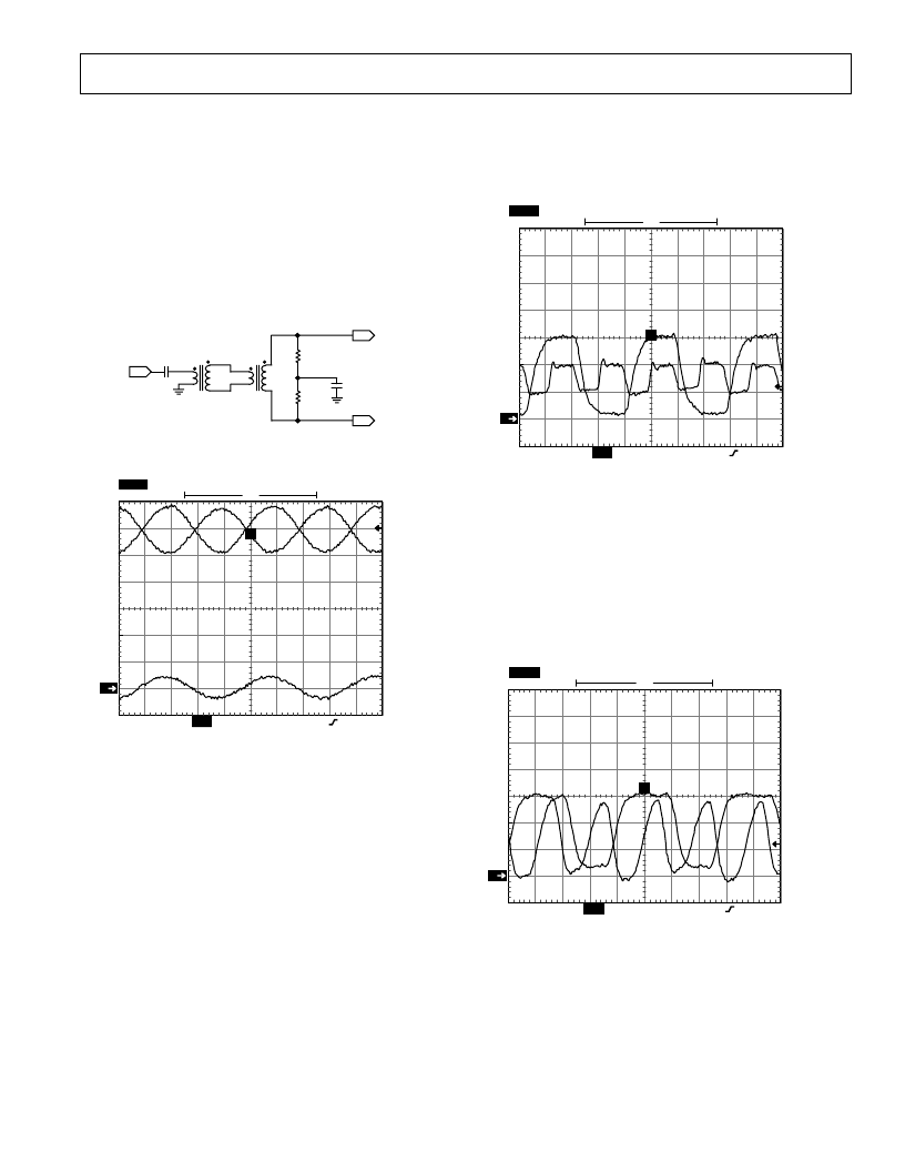
Analog Inputs
The evaluation board accepts a 2 V p-p analog input signal at
SMB connector P2. This single-ended signal is ac-coupled by
capacitor C11 and drives a wideband RF transformer T1 (Mini-
Circuits ADT1-1WT) that converts the single-ended signal to a
differential signal. (
The AD9432 should be driven differentially to
provide optimum performance
.) The evaluation board is shipped
with termination resistors R4, R5, which provide the effective
50
termination impedance; input termination resistor R10 is
optional. Note: The second harmonic distortion that some RF
transformers tend to introduce at high frequencies can be reduced
by coupling two transformers in series as shown in Figure 29
below. (Improvements on the order of 3 dB–4 dB can be realized.)
IN
TO AIN+
R1
25
R2
25
C1
0.1 F
TO AIN
–
T2
T1
C2
0.1 F
Figure 29. Improving Second Harmonic Distortion
Performance
CH2
CH1
CH3
500mV
2.00V
500mV
M 5.00ns CH1
3.00V
STOP:
TEK
5.00GS/s
[T]
14 ACQS
C1 MAX
3.4V
C1 MIN
2.5mV
C1 FREQ
49.995MHz
LOW SIGNAL
AMPLITUDE
T
2
Figure 30. Analog Input Levels
The full-scale analog inputs to the ADC should be two 1 V p-p
signals 180 degrees out of phase with each other as shown in
Figure 30. The analog inputs are dc biased by two on-chip
resistor dividers that set the common-mode voltage to approxi-
mately 0.6
×
VCC (0.6
×
5 = 3 V). AIN+ and AIN– each vary
between 2.5 V and 3.5 V as shown in the two upper traces in Fig-
ure 30. The lower trace is the input at SMB P2 (
on a 2 V/div scale
).
Encode
The encode input to the board is at SMB connector P3. The
(>1 V p-p) input is ac-coupled and drives two high-speed differ-
ential line receivers (MC10EL16). These receivers provide
subnanosecond rise times at their outputs—a requirement for
the ADC clock inputs for optimum performance. The EL16
outputs are PECL levels and must be ac-coupled to meet the
common-mode dc levels required at the AD9432 encode inputs.
A PECL/TTL translator (MC100ELT23), provides the clocks
required at the output latches, DAC, and 37-pin connector.
Note: Jitter performance on the clock source is critical at this
performance level; a stable, crystal-controlled signal generator is
used to generate all of the ADC performance plots. Figure 31
shows the Encode+ clock at the ADC. The 3 V Latch clock
generated on the card is also shown in the plot.
CH2
2
CH1
1.00V
1.00V
M 5.00ns
CH1
1.20V
[T]
86 ACQS
C1 MAX
2.33V
C1 MIN
810mV
C1 FREQ
106.3167MHz
LOW
SIGNAL
AMPLITUDE
T
STOP:
TEK
5.00GS/s
Figure 31. Encode+ Clock and Latch Clock
DATA OUTPUTS
The ADC digital outputs are latched on the board by two 574s,
the latch outputs are available at the 37-pin connector at Pins
25–36. A latch output clock (data ready) is available at Pin 21,
with the complement at Pin 2. There are series termination
resistors on the data and clock outputs. These can be changed if
required to accommodate different loading situations. Figure
32 shows a data bit switching and output clock (DR) at the
connector.
CH2
2
CH1
1.00V
1.00V
M 5.00ns
CH1
1.20V
[T]
265 ACQS
C1 MAX
3.06V
C1 MIN
–
390mV
C1 FREQ
105.4562MHz
T
STOP:
TEK
5.00GS/s
Figure 32. Data Bit and Clock at 37-Pin Connector
REFERENCE
The AD9432 has an on-chip reference of 2.5 V available at
VREFOUT (Pin 46). Most applications will simply tie this
output to the VREFIN input (Pin 45). This is accomplished
jumping E4 to E6 on the board. An external voltage reference
can drive the VREFIN pin if desired by strapping E4 to E3 and
placing an AD780 voltage reference on the board (not supplied).
相關PDF資料 |
PDF描述 |
|---|---|
| AD9432BST-105 | 12-Bit, 80 MSPS/105 MSPS A/D Converter |
| AD9432BSQ-105 | 12-Bit, 80 MSPS/105 MSPS A/D Converter |
| AD9432BSQ-80 | 12-Bit, 80 MSPS/105 MSPS A/D Converter |
| AD9432 | 12-Bit, 100 MSPS A/D Converter(100MSPS,12位A/D轉換器) |
| AD9433BSQ-125 | 12-Bit, 105 MSPS/125 MSPS IF Sampling A/D Converter |
相關代理商/技術參數 |
參數描述 |
|---|---|
| AD9432BSTZ105 | 制造商:Analog Devices 功能描述:AD9432BSTZ105 |
| AD9432BSTZ-105 | 功能描述:IC ADC 12BIT 105MSPS 52-LQFP RoHS:是 類別:集成電路 (IC) >> 數據采集 - 模數轉換器 系列:- 其它有關文件:TSA1204 View All Specifications 標準包裝:1 系列:- 位數:12 采樣率(每秒):20M 數據接口:并聯 轉換器數目:2 功率耗散(最大):155mW 電壓電源:模擬和數字 工作溫度:-40°C ~ 85°C 安裝類型:表面貼裝 封裝/外殼:48-TQFP 供應商設備封裝:48-TQFP(7x7) 包裝:Digi-Reel® 輸入數目和類型:4 個單端,單極;2 個差分,單極 產品目錄頁面:1156 (CN2011-ZH PDF) 其它名稱:497-5435-6 |
| AD9432BSTZ-105 | 制造商:Analog Devices 功能描述:IC 12-BIT ADC |
| AD9432BSTZ-1051 | 制造商:AD 制造商全稱:Analog Devices 功能描述:12-Bit, 80 MSPS/105 MSPS ADC |
| AD9432BSTZ-80 | 功能描述:IC ADC 12BIT 80MSPS 52-LQFP RoHS:是 類別:集成電路 (IC) >> 數據采集 - 模數轉換器 系列:- 標準包裝:1 系列:- 位數:14 采樣率(每秒):83k 數據接口:串行,并聯 轉換器數目:1 功率耗散(最大):95mW 電壓電源:雙 ± 工作溫度:0°C ~ 70°C 安裝類型:通孔 封裝/外殼:28-DIP(0.600",15.24mm) 供應商設備封裝:28-PDIP 包裝:管件 輸入數目和類型:1 個單端,雙極 |
發布緊急采購,3分鐘左右您將得到回復。