- 您現在的位置:買賣IC網 > PDF目錄373964 > AD9630AR-REEL (ANALOG DEVICES INC) ECONOLINE: REC3-S_DRW(Z)/H4,H6 - Safety standards and approval: EN 60950 certified, rated for 250VAV (LVD test report)- Applied for Ul 1950 Component Recognised Certification- 3W DIP Package- 4kVDC & 6kVDC Isolation- Regulated Output- Continuous Short Circiut Protection Auto-Restarting PDF資料下載
參數資料
| 型號: | AD9630AR-REEL |
| 廠商: | ANALOG DEVICES INC |
| 元件分類: | 運動控制電子 |
| 英文描述: | ECONOLINE: REC3-S_DRW(Z)/H4,H6 - Safety standards and approval: EN 60950 certified, rated for 250VAV (LVD test report)- Applied for Ul 1950 Component Recognised Certification- 3W DIP Package- 4kVDC & 6kVDC Isolation- Regulated Output- Continuous Short Circiut Protection Auto-Restarting |
| 中文描述: | BUFFER AMPLIFIER, PDSO8 |
| 封裝: | SOIC-8 |
| 文件頁數: | 3/7頁 |
| 文件大小: | 101K |
| 代理商: | AD9630AR-REEL |
AD9630
–3–
REV. B
ABSOLUTE MAXIMUM RATINGS
1
Supply Voltages (
±
V
S
) . . . . . . . . . . . . . . . . . . . . . . . . . . .
±
7 V
Continuous Output Current
2
. . . . . . . . . . . . . . . . . . . . . 70 mA
Temperature Range over Which Specifications Apply
AD9630AN/AR . . . . . . . . . . . . . . . . . . . . . –40
°
C to +85
°
C
Lead Soldering Temperature (10 sec) . . . . . . . . . . . . . +300
°
C
Storage Temperature
AD9630AN/AR . . . . . . . . . . . . . . . . . . . . –65
°
C to +150
°
C
Junction Temperature
3
AD9630AN/AR . . . . . . . . . . . . . . . . . . . . . . . . . . . . +150
°
C
NOTES
1
Absolute maximum ratings are limiting values to be applied individually, and
beyond which the serviceability of the circuit may be impaired. Functional
operability is not necessarily implied. Exposure to absolute maximum rating
conditions for an extended period of time may affect device reliability.
2
Output is short-circuit protected to ground, but not to supplies. Prolonged short
circuit to ground may affect device reliability.
3
Typical thermal impedances (part soldered onto board): Plastic DIP (N):
θ
JA
=
110
°
C/W;
θ
JC
= 30
°
C/W; SOIC (R):
θ
JA
= 155
°
C/W;
θ
JC
= 40
°
C/W.
ORDERING GUIDE
Temperature
Range
Package
Description
Package
Option
Model
AD9630AN
AD9630AR
AD9630AR-REEL –40
°
C to +85
°
C 13
"
Tape and Reel SO-8
–40
°
C to +85
°
C 8-Lead Plastic DIP N-8
–40
°
C to +85
°
C 8-Lead SOIC
SO-8
CAUTION
ESD (electrostatic discharge) sensitive device. Electrostatic charges as high as 4000 V readily
accumulate on the human body and test equipment and can discharge without detection.
Although the AD9630 features proprietary ESD protection circuitry, permanent damage may
occur on devices subjected to high energy electrostatic discharges. Therefore, proper ESD
precautions are recommended to avoid performance degradation or loss of functionality.
EXPLANATION OF TEST LEVELS
Test Level
I
100% Production tested.
II
100% Production tested at +25
°
C and sample tested at
specified temperatures. AC testing of AN and AR grades
done on sample basis only.
III Sample tested only.
IV Parameter is guaranteed by design and characterization
testing.
V
Typical value.
VI S Versions are 100% production tested at temperature
extremes. Other grades are sample tested at extremes.
1
2
3
4
8
7
6
5
TOP VIEW
(Not to Scale)
NC = NO CONNECT
AD9630
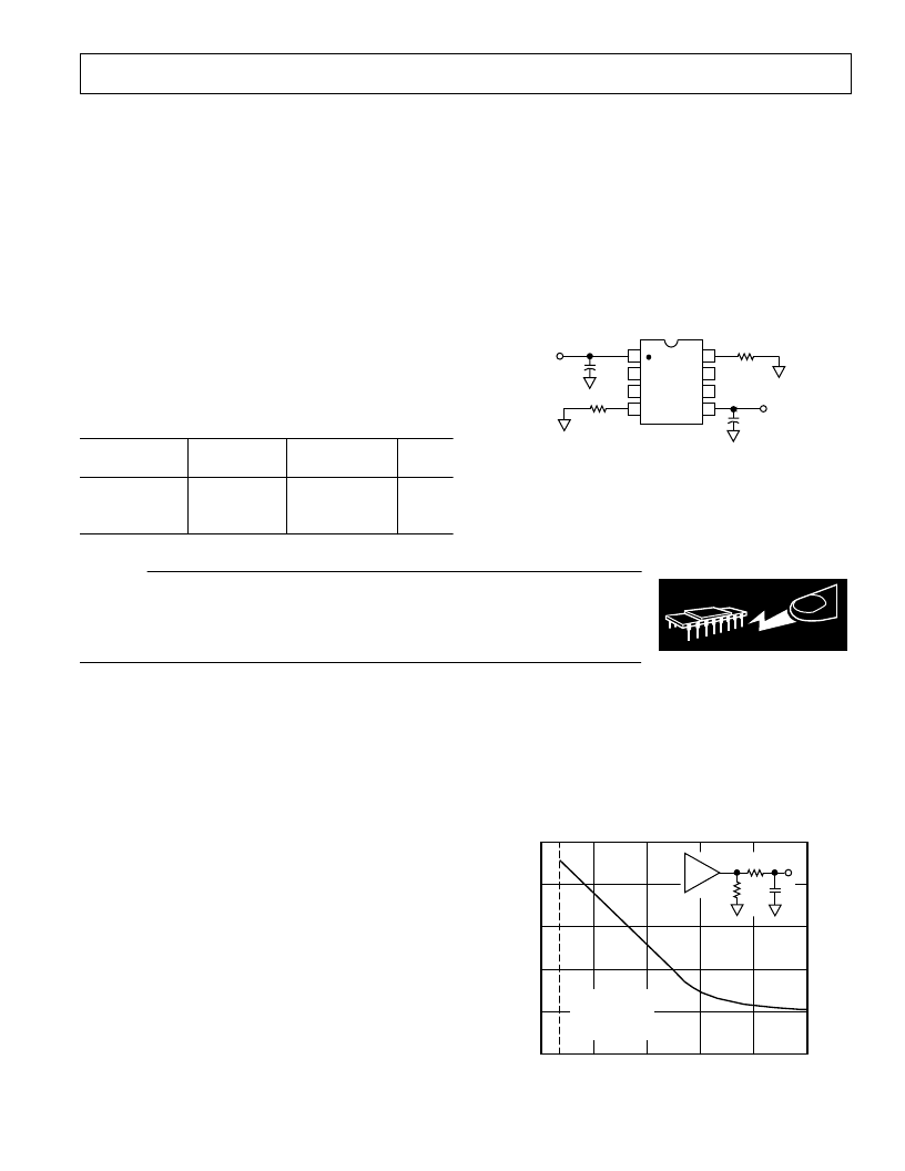
NC
NC
NC
NC
100
(5%, 0.25W)
24
V
(5%, 0.25W)
+5V
–5.2V
0.1
m
F
0.1
m
F
AD9630 Burn-In Circuit
THEORY OF OPERATION
The AD9630 is a wide-bandwidth, closed-loop, unity-gain
buffer that makes use of a new voltage-feedback architecture.
This architecture brings together wide bandwidth and high slew
rate along with exceptional dc linearity. Most previous wide-
bandwidth buffers achieved their bandwidth by utilizing an
open-loop topology which sacrificed both dc linearity and fre-
quency distortion when driven into low load impedances. The
design’s high loop correction factor radically improves dc lin-
earity and distortion characteristics without diminishing
bandwidth. This, in combination with high slew rate, results in
exceptionally low distortion over a wide frequency range.
The AD9630 is an excellent choice to drive high speed and high
resolution analog-to-digital converters. Its output stage is de-
signed to drive high speed flash converters with minimal or no
series resistance. A current booster built into the output driver
helps to maintain low distortion.
Parasitic or load capacitance (>7 pF) connected directly to the
AD9630 output will result in frequency peaking. A small series
resistor (R
S
) connected between the buffer output and capaci-
tive load will negate this effect. Figure 1 shows the optimal value
of R
S
as a function of C
L
to obtain the flattest frequency re-
sponse. Figure 2 illustrates frequency response for various
capacitive loads utilizing the recommended R
S
.
C
L
– pF
50
40
00
100
20
R
S
V
40
60
80
30
20
10
7
R
S
C
L
200
V
"R"
NO
R
S
NEEDED
WHEN
C
L
<
7pF;
FOR
C
L
>
30pF,
"R"
CAN
BE
OMITTED
Figure 1. Recommended R
S
vs. C
L
WARNING!
ESD SENSITIVE DEVICE
相關PDF資料 |
PDF描述 |
|---|---|
| AD9630* | Low Distortion 750 MHz Closed-Loop Buffer Amp |
| AD9631AN | Ultralow Distortion, Wide Bandwidth Voltage Feedback Op Amps |
| AD9631AR | Ultralow Distortion, Wide Bandwidth Voltage Feedback Op Amps |
| AD9632 | Ultralow Distortion, Wide Bandwidth Voltage Feedback Op Amps |
| AD9632-EB | Ultralow Distortion, Wide Bandwidth Voltage Feedback Op Amps |
相關代理商/技術參數 |
參數描述 |
|---|---|
| AD9630SQ | 制造商:未知廠家 制造商全稱:未知廠家 功能描述:Analog Buffer/Voltage Follower |
| AD9630SQ/883B | 制造商:Rochester Electronics LLC 功能描述:- Bulk 制造商:Analog Devices 功能描述: |
| AD9630SZ/883B | 制造商:Rochester Electronics LLC 功能描述:- Bulk |
| AD9631 | 制造商:AD 制造商全稱:Analog Devices 功能描述:Ultralow Distortion, Wide Bandwidth Voltage Feedback Op Amps |
| AD9631_03 | 制造商:AD 制造商全稱:Analog Devices 功能描述:Ultralow Distortion, Wide Bandwidth Voltage Feedback Op Amps |
發布緊急采購,3分鐘左右您將得到回復。