- 您現在的位置:買賣IC網 > PDF目錄373968 > AD9816-EB (Analog Devices, Inc.) Complete 12-Bit 6 MSPS CCD/CIS Signal Processor PDF資料下載
參數資料
| 型號: | AD9816-EB |
| 廠商: | Analog Devices, Inc. |
| 英文描述: | Complete 12-Bit 6 MSPS CCD/CIS Signal Processor |
| 中文描述: | 完整的12位6 MSPS的防治荒漠化公約/ CIS信號處理器 |
| 文件頁數: | 10/16頁 |
| 文件大小: | 171K |
| 代理商: | AD9816-EB |
AD9816
–10–
REV. A
Table II. 3-Channel Selection
MUX Register Bits
6
5
Channel Sequence
0
1
1
0
Red, Green, Blue
Blue, Green, Red
Table III. 1-Channel Selection
MUX Register Bits
4
3
2
Channel
0
0
1
0
1
0
1
0
0
Red
Green
Blue
The offset is variable from –100 mV to +100 mV, and is applied
at the output of the CDS, before the PGA. The resolution is
8 bits, and a sign magnitude coding scheme is used. Table IV
shows the offset voltage that corresponds to the register value.
7 6 5 4 3 2 1 0
D0 (LSB)
D1
D2
D3
D4
D5
D6
D7 (MSB)
Figure 9. Offset Registers for Red, Green and Blue
Channels
Table IV. Offset Adjustment
Offset Register
Offset Voltage
0111 1111 (LSB)
.
.
.
0000 0001
0000 0000
1000 0000
1000 0001
.
.
.
1111 1111
+100 mV
.
.
.
+0.8 mV
0.0 mV
0.0 mV
–0.8 mV
.
.
.
–100 mV
The PGA is used for correcting color imbalance and for fine
adjustment of the input span before the ADC. Gain is variable
from 1
×
to 6
×
(0 dB to 15.5 dB) with 8-bit resolution. An all
“zeros” word (00 . . . 0) corresponds to the minimum gain, and
an all “ones” word (11 . . . 1) corresponds to the maximum
gain. The gain of the PGA increases linearly as the gain word
increases, and can be calculated by the following equation:
PGA Gain
= 1 + (
Gain Code
/51.2)
where
Gain Code
varies from 0 to 255. For more information,
refer to
the Circuit Descriptions section.
7 6 5 4 3 2 1 0
D0 (LSB)
D1
D2
D3
D4
D5
D6
D7 (MSB)
Figure 10. PGA Registers for Red, Green and Blue
Channels
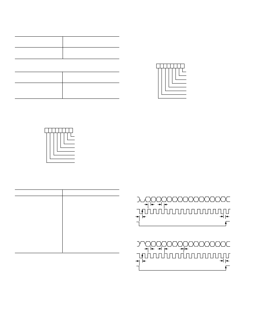
SERIAL TIMING
The 3-wire serial interface timing is shown below. To write to
the AD9816, SLOAD is first taken low. Next, a total of 16 bits
are sent to SDATA, which get latched into the AD9816 on the
rising edges of SCLK. Additional SCLK pulses will be ignored.
The first bit, R/
W
, should be low to specify a write operation.
The next three bits, A2–A0, are the address bits to specify the
destination register for the data word D7–D0. After all 16 bits
have been clocked, SLOAD is taken high, which internally
latches the data to the appropriate register. The read operation
also starts by taking SLOAD low. First, a one is written to R/
W
,
to specify a read operation. Next, the three Address Bits A2–A0
are written to specify the register that will be read. On the 8th
SCLK falling edge, SDATA will begin to output the informa-
tion from the desired register. After all eight data bits have been
read, SLOAD is taken back high.
t
DH
t
DS
t
LS
t
LH
SDATA
SCLK
SLOAD
R/Wb
A2
A1 A0
D7 D6 D5
D4 D3 D2
D1
D0
Figure 11. Write Operation Timing
t
DH
t
DS
t
LS
t
LH
SDATA
SCLK
SLOAD
R/Wb
A2
A1 A0
D7 D6 D5
D4 D3 D2
D1
D0
t
RDV
Figure 12. Read Operation Timing
相關PDF資料 |
PDF描述 |
|---|---|
| AD9816JS | Complete 12-Bit 6 MSPS CCD/CIS Signal Processor |
| AD9816JS-80010 | Complete 12-Bit 6 MSPS CCD/CIS Signal Processor |
| AD9816 | Complete 12-Bit 6 MSPS CCD/CIS Signal Processor(12位的采樣速率為6MSPS的CCD/CIS信號處理器) |
| AD9821 | Complete 12-Bit 40 MSPS Imaging Signal Processor |
| AD9821KST | Complete 12-Bit 40 MSPS Imaging Signal Processor |
相關代理商/技術參數 |
參數描述 |
|---|---|
| AD9816JS | 制造商:Analog Devices 功能描述:AFE VID 1ADC 12-BIT 5V/5V 44MQFP - Bulk 制造商:Rochester Electronics LLC 功能描述: |
| AD9816JS-80010 | 制造商:AD 制造商全稱:Analog Devices 功能描述:Complete 12-Bit 6 MSPS CCD/CIS Signal Processor |
| AD9816JSRL | 制造商:Rochester Electronics LLC 功能描述:- Tape and Reel 制造商:Analog Devices 功能描述: |
| AD9821 | 制造商:AD 制造商全稱:Analog Devices 功能描述:Complete 12-Bit 40 MSPS Imaging Signal Processor |
| AD9821KST | 制造商:Analog Devices 功能描述:AFE Video 1ADC 12-Bit 3.3V 48-Pin LQFP 制造商:Rochester Electronics LLC 功能描述:12 BIT 40 MSPS IMAGING SIGNAL PROCESSOR - Bulk |
發布緊急采購,3分鐘左右您將得到回復。