- 您現在的位置:買賣IC網 > PDF目錄373968 > AD9831AST (ANALOG DEVICES INC) CMOS Complete DDS PDF資料下載
參數資料
| 型號: | AD9831AST |
| 廠商: | ANALOG DEVICES INC |
| 元件分類: | 數字信號處理外設 |
| 英文描述: | CMOS Complete DDS |
| 中文描述: | 16-BIT, DSP-NUM CONTROLLED OSCILLATOR, PQFP48 |
| 封裝: | TQFP-48 |
| 文件頁數: | 10/16頁 |
| 文件大小: | 172K |
| 代理商: | AD9831AST |
AD9831
–10–
REV. A
Numerical Controlled Oscillator + Phase Modulator
T his consists of two frequency select registers, a phase accumu-
lator and four phase offset registers. T he main component of the
NCO is a 32-bit phase accumulator which assembles the phase
component of the output signal. Continuous time signals have a
phase range of 0 to 2
π
. Outside this range of numbers, the
sinusoid functions repeat themselves in a periodic manner. T he
digital implementation is no different. T he accumulator simply
scales the range of phase numbers into a multibit digital word.
T he phase accumulator in the AD9831 is implemented with 32
bits. T herefore, in the AD9831, 2
π
= 2
32
. Likewise, the
Phase
term is scaled into this range of numbers 0 <
Phase
< 2
32
– 1.
Making these substitutions into the equation above
f
=
Phase
×
f
MCLK
/2
32
where 0 <
Phase
< 2
32
With a clock signal of 25 MHz and a phase word of 051EB852
hex
f
= 51EB852
×
25
MHz
/2
32
= 0.500000000465
MHz
T he input to the phase accumulator (i.e., the phase step) can be
selected either from the FREQ0 Register or FREQ1 Register
and this is controlled by the FSELECT pin. NCOs inherently
generate continuous phase signals, thus avoiding any output
discontinuity when switching between frequencies.
Following the NCO, a phase offset can be added to perform
phase modulation using the 12-bit PHASE Registers. T he con-
tents of this register are added to the most significant bits of the
NCO. T he AD9831 has four PHASE registers, the resolution
of these registers being 2
π
/4096.
Sine Look-Up T able (LUT )
T o make the output useful, the signal must be converted from
phase information into a sinusoidal value. Since phase informa-
tion maps directly into amplitude, a ROM LUT converts the
phase information into amplitude. T o do this, the digital phase
information is used to address a sine ROM LUT . Although the
NCO contains a 32-bit phase accumulator, the output of the
NCO is truncated to 12 bits. Using the full resolution of the
phase accumulator is impractical and unnecessary as this would
require a look-up table of 2
32
entries.
It is necessary only to have sufficient phase resolution in the
LUT s such that the dc error of the output waveform is domi-
nated by the quantization error in the DAC. T his requires the
look-up table to have two more bits of phase resolution than the
10-bit DAC.
Digital-to-Analog Converter
T he AD9831 includes a high impedance current source 10-bit
DAC, capable of driving a wide range of loads at different
speeds. Full-scale output current can be adjusted, for optimum
power and external load requirements, through the use of a
single external resistor (R
SET
).
T he DAC is configured for single ended operation. T he load
resistor can be any value required, as long as the full-scale volt-
age developed across it does not exceed the voltage compliance
range. Since full-scale current is controlled by R
SET
, adjust-
ments to R
SET
can balance changes made to the load resistor.
However, if the DAC full-scale output current is significantly
less than 4 mA, the DAC’s linearity may degrade.
CIRCUIT DE SCRIPT ION
T he AD9831 provides an exciting new level of integration for
the RF/Communications system designer. T he AD9831 com-
bines the Numerical Controlled Oscillator (NCO), SINE Look-
Up T able, Frequency and Phase Modulators, and a Digital-to-
Analog Converter on a single integrated circuit.
T he internal circuitry of the AD9831 consists of three main
sections. T hese are:
Numerical Controlled Oscillator (NCO) + Phase Modulator
SINE Look-Up T able
Digital-to-Analog Converter
T he AD9831 is a fully integrated Direct Digital Synthesis
(DDS) chip. T he chip requires one reference clock, one low
precision resistor and eight decoupling capacitors to provide
digitally created sine waves up to 12.5 MHz. In addition to the
generation of this RF signal, the chip is fully capable of a broad
range of simple and complex modulation schemes. T hese
modulation schemes are fully implemented in the digital domain
allowing accurate and simple realization of complex modulation
algorithms using DSP techniques.
T HE ORY OF OPE RAT ION
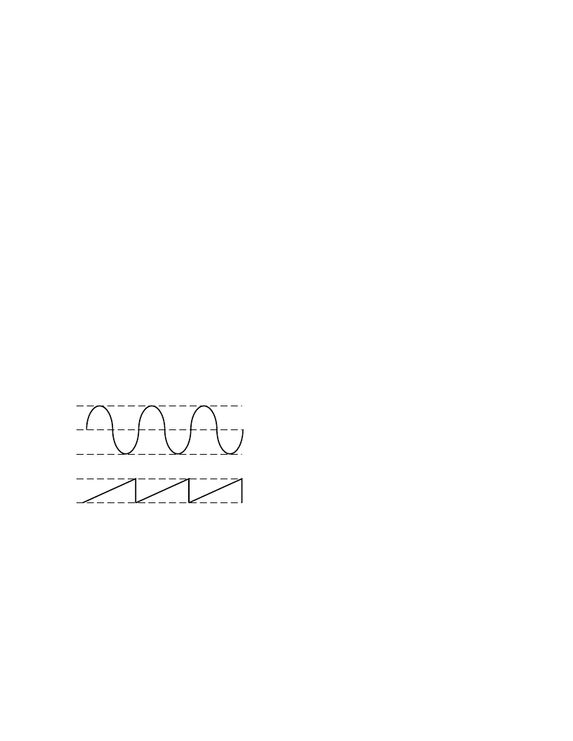
Sine waves are typically thought of in terms of their magnitude
form a(t) = sin (
ω
t). However, these are nonlinear and not easy
to generate except through piece wise construction. On the
other hand, the angular information is linear in nature. T hat is,
the phase angle rotates through a fixed angle for each unit of
time. T he angular rate depends on the frequency of the signal
by the traditional rate of
ω
= 2
π
f.
MAGNITUDE
PHASE
+1
0
–1
2
π
0
Figure 21. Sine Wave
K nowing that the phase of a sine wave is linear and given a
reference interval (clock period), the phase rotation for that
period can be determined.
Phase
=
ωδ
t
Solving for
ω
ω
=
Phase
/
δ
t = 2
π
f
Solving for f and substituting the reference clock frequency for
the reference period (1/f
MCLK
=
δ
t)
f
=
Phase
×
f
MCLK
/2
π
T he AD9831 builds the output based on this simple equation.
A simple DDS chip can implement this equation with three
major subcircuits.
相關PDF資料 |
PDF描述 |
|---|---|
| AD9832 | CMOS Complete DDS |
| AD9832BRU | CMOS Complete DDS |
| AD9833 | +2.5 V to +5.5 V, 25 MHz Low Power CMOS Complete DDS |
| AD9833BRM | +2.5 V to +5.5 V, 25 MHz Low Power CMOS Complete DDS |
| AD9834 | Low Power, +2.3 V to +5.5 V, 50 MHz Complete DDS |
相關代理商/技術參數 |
參數描述 |
|---|---|
| AD9831AST-REEL | 制造商:Analog Devices 功能描述:Direct Digital Synthesizer 25MHz 1-DAC 10-Bit Parallel 48-Pin LQFP T/R 制造商:Rochester Electronics LLC 功能描述:25 MHZ +5V/+3V, 10-BIT DDS DAC I.C. - Tape and Reel |
| AD9831ASTZ | 功能描述:IC DDS 10BIT 25MHZ CMOS 48-LQFP RoHS:是 類別:集成電路 (IC) >> 接口 - 直接數字合成 (DDS) 系列:- 產品變化通告:Product Discontinuance 27/Oct/2011 標準包裝:2,500 系列:- 分辨率(位):10 b 主 fclk:25MHz 調節字寬(位):32 b 電源電壓:2.97 V ~ 5.5 V 工作溫度:-40°C ~ 85°C 安裝類型:表面貼裝 封裝/外殼:16-TSSOP(0.173",4.40mm 寬) 供應商設備封裝:16-TSSOP 包裝:帶卷 (TR) |
| AD9831ASTZKL1 | 制造商:Rochester Electronics LLC 功能描述: 制造商:Analog Devices 功能描述: |
| AD9831ASTZ-REEL | 功能描述:IC DDS 10BIT 25MHZ CMOS 48TQFP RoHS:是 類別:集成電路 (IC) >> 接口 - 直接數字合成 (DDS) 系列:- 產品變化通告:Product Discontinuance 27/Oct/2011 標準包裝:2,500 系列:- 分辨率(位):10 b 主 fclk:25MHz 調節字寬(位):32 b 電源電壓:2.97 V ~ 5.5 V 工作溫度:-40°C ~ 85°C 安裝類型:表面貼裝 封裝/外殼:16-TSSOP(0.173",4.40mm 寬) 供應商設備封裝:16-TSSOP 包裝:帶卷 (TR) |
| AD9832 | 制造商:AD 制造商全稱:Analog Devices 功能描述:CMOS Complete DDS |
發布緊急采購,3分鐘左右您將得到回復。