- 您現在的位置:買賣IC網 > PDF目錄373968 > AD9844 (Analog Devices, Inc.) Complete 12-Bit 20 MSPS CCD Signal Processor PDF資料下載
參數資料
| 型號: | AD9844 |
| 廠商: | Analog Devices, Inc. |
| 英文描述: | Complete 12-Bit 20 MSPS CCD Signal Processor |
| 中文描述: | 完整的12位20 MSPS的CCD信號處理器 |
| 文件頁數: | 12/16頁 |
| 文件大小: | 169K |
| 代理商: | AD9844 |
AD9844A
–12–
REV. 0
2dB TO 36dB
CLPDM
CCDIN
12
DIGITAL
FILTERING
CLPOB
DC RESTORE
INPUT OFFSET
CLAMP
OPTICAL BLACK
CLAMP
0 TO 255 LSB
0.1 F
DOUT
12-BIT
ADC
VGA
8-BIT
DAC
8
VGA GAIN
REGISTER
10
CDS
–
2dB TO +10dB
INTERNAL
V
REF
2V FULL SCALE
CDS GAIN
REGISTER
6
CLAMP LEVEL
REGISTER
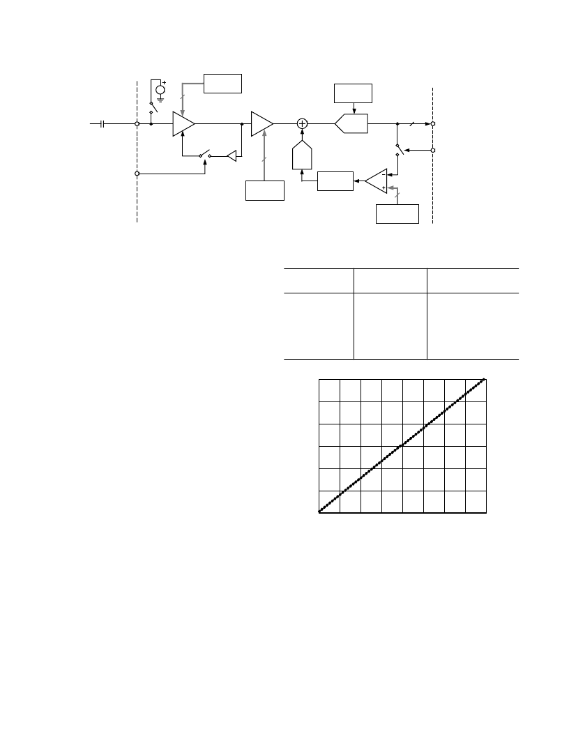
Figure 11. CCD-Mode Block Diagram
CIRCUIT DESCRIPTION AND OPERATION
The AD9844A signal processing chain is shown in Figure 11.
Each processing step is essential in achieving a high-quality
image from the raw CCD pixel data.
DC Restore
To reduce the large dc offset of the CCD output signal, a
dc-restore circuit is used with an external 0.1
μ
F series-coupling
capacitor. This restores the dc level of the CCD signal to approxi-
mately 1.5 V, to be compatible with the 3 V single supply of
the AD9844A.
Correlated Double Sampler
The CDS circuit samples each CCD pixel twice to extract the
video information and reject low-frequency noise. The timing
shown in Figure 5 illustrates how the two CDS clocks, SHP
and SHD, are used to sample the reference level and data level
of the CCD signal respectively. The CCD signal is sampled on the
rising edges of SHP and SHD. Placement of these two clock
signals is critical in achieving the best performance from the CCD.
An internal SHP/SHD delay (t
ID
) of 3 ns is caused by internal
propagation delays.
The CDS stage has a default gain of 4 dB, but uses a unique
architecture that allows the CDS gain to be varied. Using the
CDS Gain Register, the gain is programmable from –2 dB to
+10 dB in 64 steps, using two’s complement coding. The CDS
Gain curve is shown in Figure 12. To change the gain of the
CDS using the CDS Gain Register, the Control Register bit D3
must be set high (CDS Gain Enabled). The default gain setting
when bit Control Register Bit D3 is low (CDS Gain Disabled) is
4 dB. See Tables V and VI for more details.
A CDS gain of 4 dB provides some front-end signal gain and
improves the overall signal-to-noise ratio. This gain setting
works very well in most applications, and the CCD-Mode
Specifications use this default gain setting. However, the CDS
gain may be varied to optimize the AD9844A operation in a
particular application. Increased CDS gain can be useful with
low output level CCDs, while decreased CDS gain allows the
AD9844A to accept CCD signal swings greater than 1 V p-p.
Table VII summarizes some example CDS gain settings for
different maximum signal swings. The CDS Gain Register may
also be used “on the fly” to provide a +6 dB boost or –6 dB
attenuation when setting exposure levels. It is best to keep the
CDS
output
level
from exceeding 1.5 V~1.6 V.
Table VII. Example CDS Gain Settings
Recommended
Gain Range
Max Input Signal
Register Code Range
250 mV p-p
500 mV p-p
800 mV p-p
1 V p-p
1.25 V p-p
1.5 V p-p
8 to 10 dB
6 to 8 dB
4 to 6 dB
2 to 4 dB
0 to 2 dB
–2 to 0 dB
21 to 31
10 to 21
63 to 10
53 to 63
42 to 53
32 to 42
CDS GAIN REGISTER CODE
10
32
C
40
48
56
0
8
16
24
31
8
6
4
2
0
-2
(100000)
(011111)
Figure 12. CDS Gain Curve
相關PDF資料 |
PDF描述 |
|---|---|
| AD9844A | Complete 12-Bit 20 MSPS CCD Signal Processor |
| AD9844AJST | Complete 12-Bit 20 MSPS CCD Signal Processor |
| AD9845B | Complete 12-Bit 30 MSPS CCD Signal Processor |
| AD9845BJST | Complete 12-Bit 30 MSPS CCD Signal Processor |
| AD9845 | Complete 12-Bit 30 MSPS CCD Signal Processor |
相關代理商/技術參數 |
參數描述 |
|---|---|
| AD9844A | 制造商:AD 制造商全稱:Analog Devices 功能描述:Complete 12-Bit 20 MSPS CCD Signal Processor |
| AD9844AJST | 制造商:Analog Devices 功能描述:AFE Video 1ADC 12-Bit 3.3V 48-Pin LQFP 制造商:Analog Devices 功能描述:AFE VID 1ADC 12-BIT 3.3V 48LQFP - Bulk 制造商:Rochester Electronics LLC 功能描述:12 BIT 20 MHZ ANALOG FRONT END - Tape and Reel |
| AD9844AJSTRL | 制造商:Analog Devices 功能描述:AFE Video 1ADC 12-Bit 3.3V 48-Pin LQFP T/R 制造商:Analog Devices 功能描述:AFE VID 1ADC 12-BIT 3.3V 48LQFP - Tape and Reel 制造商:Rochester Electronics LLC 功能描述:12 BIT 20 MHZ ANALOG FRONT END - Tape and Reel |
| AD9844AJSTZ | 制造商:Analog Devices 功能描述:AFE Video 1ADC 12-Bit 3.3V 48-Pin LQFP 制造商:Analog Devices 功能描述:12 BIT 20 MHz ANALOG FRONT END |
| AD9844-EB | 制造商:Analog Devices 功能描述: |
發布緊急采購,3分鐘左右您將得到回復。