- 您現在的位置:買賣IC網 > PDF目錄373973 > AD9995 (Analog Devices, Inc.) 12-Bit CCD Signal Processor with Precision Timing ⑩ Generator PDF資料下載
參數資料
| 型號: | AD9995 |
| 廠商: | Analog Devices, Inc. |
| 英文描述: | 12-Bit CCD Signal Processor with Precision Timing ⑩ Generator |
| 中文描述: | 12位CCD信號處理器與精密計時⑩發生器 |
| 文件頁數: | 33/60頁 |
| 文件大小: | 1593K |
| 代理商: | AD9995 |
第1頁第2頁第3頁第4頁第5頁第6頁第7頁第8頁第9頁第10頁第11頁第12頁第13頁第14頁第15頁第16頁第17頁第18頁第19頁第20頁第21頁第22頁第23頁第24頁第25頁第26頁第27頁第28頁第29頁第30頁第31頁第32頁當前第33頁第34頁第35頁第36頁第37頁第38頁第39頁第40頁第41頁第42頁第43頁第44頁第45頁第46頁第47頁第48頁第49頁第50頁第51頁第52頁第53頁第54頁第55頁第56頁第57頁第58頁第59頁第60頁
AD9995
–33–
t
PWR
2
1
3
4
5
6
7
8
9
10
11
12
t
SYNC
1V
1ST FIELD
1H
CLOCKS ACTIVE WHEN OUT CONTROL
REGISTER IS UPDATED AT VD/HD EDGE
H2/H4
H1/H3, RG, DCLK
DIGITAL
OUTPUTS
HD
(OUTPUT)
VD
(OUTPUT)
SYNC
(INPUT)
SERIAL
WRITES
CLI
(INPUT)
VDD
(INPUT)
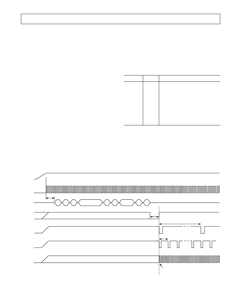
Figure 35. Recommended Power-Up Sequence and Synchronization, Master Mode
POWER-UP AND SYNCHRONIZATION
Recommended Power-Up Sequence for Master Mode
When the AD9995 is powered up, the following sequence is
recommended (refer to Figure 35 for each step). Note that a
SYNC signal is required for Master mode operation. If an exter-
nal SYNC pulse is not available, it is also possible generate an
internal SYNC pulse by writing to the SYNCPOL register, as
described in the next section.
1. Turn on power supplies for AD9995.
2. Apply the master clock input CLI.
3. Reset the internal AD9995 registers by writing a 1 to the
SW_RESET register (Addr. 0x10 in Bank 1).
4. By default, the AD9995 is in Standby3 mode. To place the
part into normal power operation, write 0x004 to the AFE
OPRMODE register (Addr. 0x00 in Bank 1).
5. Write a 1 to the BANKSELECT register (Addr. 0x7F).
This will select Register Bank 2.
6. Load Bank 2 registers with the required VPAT group,
V-sequence, and field timing information.
7. Write a 0 to the BANKSELECT register to select Bank 1.
8. By default, the internal timing core is held in a reset state
with TGCORE_RSTB register = 0. Write a 1 to the TG-
CORE_RSTB register (Addr. 0x15 in Bank 1) to start the
internal timing core operation.
9. Load the required registers to configure the high speed tim-
ing, horizontal timing, and shutter timing information.
10. Configure the AD9995 for Master mode timing by writing a
1 to the MASTER register (Addr. 0x20 in Bank 1).
11. Write a 1 to the OUT_CONTROL register (Addr. 0x11 in
Bank 1). This will allow the outputs to become active after
the next SYNC rising edge.
12. Generate a SYNC event: If SYNC is high at power-up,
bring the SYNC input low for a minimum of 100 ns.
Then bring SYNC back high. This will cause the internal
counters to reset and will start VD/HD operation. The first
VD/HD edge allows most Bank 1 register updates to occur,
including OUT_CONTROL to enable all outputs.
Table XIII. Power-Up Register Write Sequence
Address Data Description
0x10 0x01 Reset All Registers to Default Values
0x00 0x04 Power Up the AFE and CLO Oscillator
0x7F 0x01 Select Register Bank 2
0x00–0xFF VPAT, V-Sequence, and Field Timing
0x7F 0x00 Select Register Bank 1
0x15 0x01 Reset Internal Timing Core
0x30–71 Horizontal and Shutter Timing
0x20 0x01 Configure for Master Mode
0x11 0x01 Enable All Outputs after SYNC
0x13 0x01 SYNCPOL (for Software SYNC Only)
Generating Software SYNC without External SYNC Signal
If an external SYNC pulse is not available, it is possible to
generate an internal SYNC in the AD9995 by writing to the
SYNCPOL register (Addr. 0x13). If the software SYNC option is
used, the SYNC input (Pin 46) should be tied to ground (VSS).
After power-up, follow the same procedure as before for Steps
1 to 11. Then, for Step 12, instead of using the external SYNC
pulse, write a 1 to the SYNCPOL register. This will generate the
SYNC internally, and timing operation will begin.
REV. 0
相關PDF資料 |
PDF描述 |
|---|---|
| ADA4000-2ARMZ-RL | Low Cost, Precision JFET Input Operational Amplifiers |
| ADA4000-1 | Low Cost, Precision JFET Input Operational Amplifiers |
| ADA4000-1_07 | Low Cost, Precision JFET Input Operational Amplifiers |
| ADA4000-1ARZ | Low Cost, Precision JFET Input Operational Amplifiers |
| ADA4000-1ARZ-R7 | Low Cost, Precision JFET Input Operational Amplifiers |
相關代理商/技術參數 |
參數描述 |
|---|---|
| AD9995KCP | 制造商:Analog Devices 功能描述:AFE Video 1ADC 12-Bit 3V 56-Pin LFCSP EP 制造商:Rochester Electronics LLC 功能描述:12 BIT 36 MSPS ANALOG FRONT END CONVERTE - Bulk |
| AD9995KCPRL | 制造商:Analog Devices 功能描述:AFE Video 1ADC 12-Bit 3V 56-Pin LFCSP EP T/R 制造商:Rochester Electronics LLC 功能描述:- Bulk |
| AD9995KCPZ | 功能描述:IC CCD SIGNAL PROCESSOR 56-LFCSP RoHS:是 類別:集成電路 (IC) >> 接口 - 傳感器和探測器接口 系列:- 其它有關文件:Automotive Product Guide 產品培訓模塊:Lead (SnPb) Finish for COTS Obsolescence Mitigation Program 標準包裝:74 系列:- 類型:觸控式傳感器 輸入類型:數字 輸出類型:數字 接口:JTAG,串行 電流 - 電源:100µA 安裝類型:表面貼裝 封裝/外殼:20-TSSOP(0.173",4.40mm 寬) 供應商設備封裝:20-TSSOP 包裝:管件 |
| AD9995KCPZRL | 功能描述:IC CCD SIGNAL PROCESSOR 56-LFCSP RoHS:是 類別:集成電路 (IC) >> 接口 - 傳感器和探測器接口 系列:- 其它有關文件:Automotive Product Guide 產品培訓模塊:Lead (SnPb) Finish for COTS Obsolescence Mitigation Program 標準包裝:74 系列:- 類型:觸控式傳感器 輸入類型:數字 輸出類型:數字 接口:JTAG,串行 電流 - 電源:100µA 安裝類型:表面貼裝 封裝/外殼:20-TSSOP(0.173",4.40mm 寬) 供應商設備封裝:20-TSSOP 包裝:管件 |
| AD9995KCPZRL7 | 制造商:Rochester Electronics LLC 功能描述: 制造商:Analog Devices 功能描述: |
發布緊急采購,3分鐘左右您將得到回復。