- 您現(xiàn)在的位置:買賣IC網(wǎng) > PDF目錄373974 > ADA4841-2YRZ (ANALOG DEVICES INC) Low Power, Low Noise and Distortion, Rail-to-Rail Output Amplifier PDF資料下載
參數(shù)資料
| 型號(hào): | ADA4841-2YRZ |
| 廠商: | ANALOG DEVICES INC |
| 元件分類: | 運(yùn)動(dòng)控制電子 |
| 英文描述: | Low Power, Low Noise and Distortion, Rail-to-Rail Output Amplifier |
| 中文描述: | DUAL OP-AMP, 300 uV OFFSET-MAX, PDSO8 |
| 封裝: | ROHS COMPLIANT, MS-012AA, SOIC-8 |
| 文件頁(yè)數(shù): | 13/20頁(yè) |
| 文件大小: | 442K |
| 代理商: | ADA4841-2YRZ |
第1頁(yè)第2頁(yè)第3頁(yè)第4頁(yè)第5頁(yè)第6頁(yè)第7頁(yè)第8頁(yè)第9頁(yè)第10頁(yè)第11頁(yè)第12頁(yè)當(dāng)前第13頁(yè)第14頁(yè)第15頁(yè)第16頁(yè)第17頁(yè)第18頁(yè)第19頁(yè)第20頁(yè)
ADA4841-1/ADA4841-2
THEORY OF OPERATION
AMPLIFIER DESCRIPTION
The ADA4841-1/ADA4841-2 are low power, low noise,
precision voltage-feedback op amps for single or dual voltage
supply operation. The ADA4841-1/ADA4841-2 are fabricated
on ADI’s second generation XFCB process and feature trimmed
supply current and offset voltage. The 2.1 nV/√Hz voltage noise
(very low for a 1.1 mA supply current amplifier), 40 μV offset
voltage, and sub 1 μV/°C offset drift is accomplished with an
input stage made of an undegenerated PNP input pair driving a
symmetrical folded cascode. A rail-to-rail output stage provides
the maximum linear signal range possible on low voltage
supplies and has the current drive capability needed for the
relatively low resistance feedback networks required for low
noise operation. CMRR, PSRR, and open-loop gain are all
typically above 100 dB, preserving the precision performance in
a variety of configurations. Gain bandwidth is kept high for this
power level to preserve the outstanding linearity performance
for frequencies up to 100 kHz. The ADA4841-1 has a power-
down function to further reduce power consumption. All this
results in a low noise, power efficient, precision amplifier that is
well-suited for high resolution and precision applications.
Rev. C | Page 13 of 20
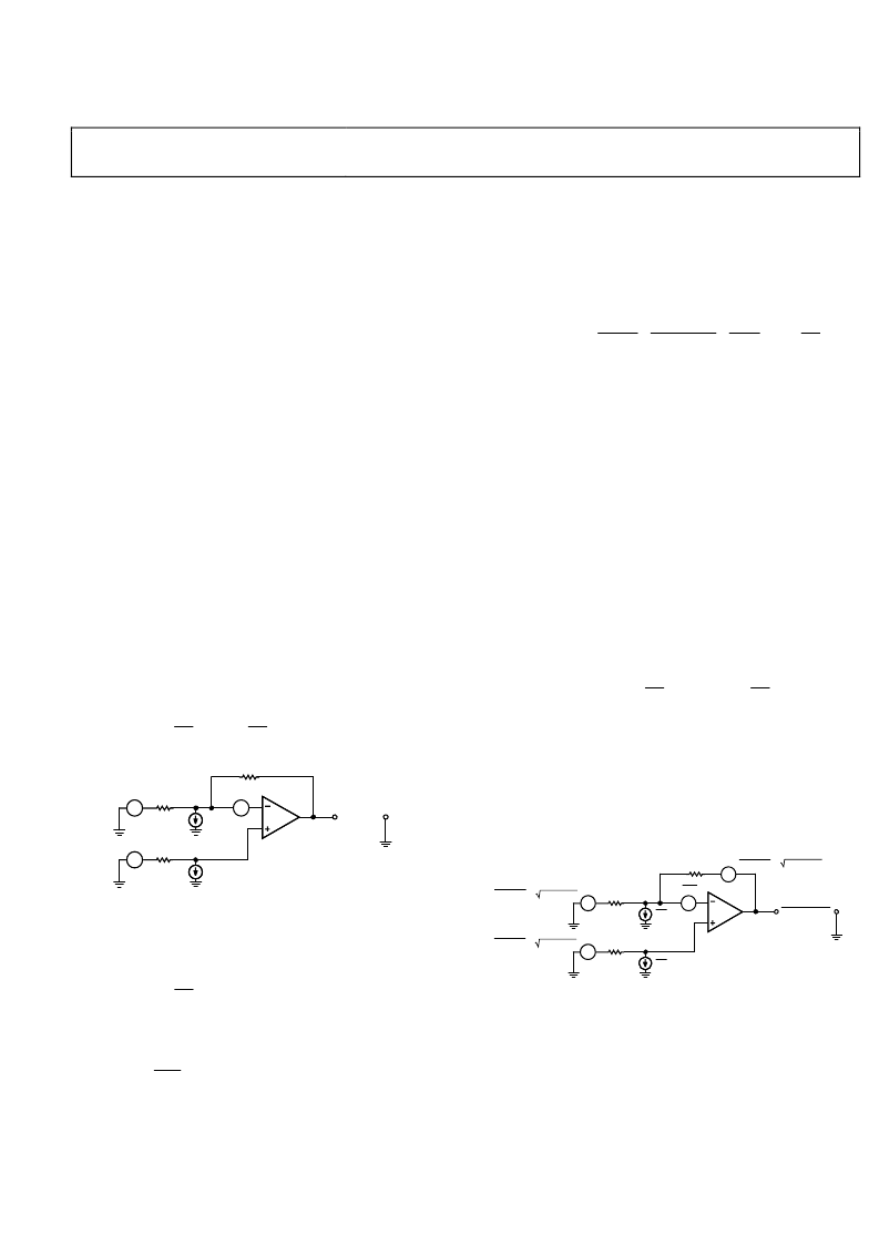
DC ERRORS
Figure 39 shows a typical connection diagram and the major dc
error sources. The ideal transfer function (all error sources set
to 0 and infinite dc gain) can be written as
IN
G
F
IP
G
F
OUT
V
V
R
R
V
R
R
×
×
+
=
1
(1)
0
R
G
– V
IN
+
R
S
– V
IP
+
I
B
+
I
B
–
+ V
OUT
–
R
F
+ V
OS
–
Figure 39. Typical Connection Diagram and DC Error Sources
This reduces to the familiar forms for inverting and
noninverting op amp gain expressions
IP
G
F
OUT
V
R
R
V
×
+
=
1
(2)
(Noninverting gain, V
IN
= 0 V)
IN
G
F
OUT
V
V
R
R
×
=
(3)
(Inverting gain, V
IP
= 0 V)
The total output voltage error is the sum of errors due to the
amplifier offset voltage and input currents. The output error
due to the offset voltage can be estimated as
=
OUT
V
ERROR
+
×
+
PSRR
+
+
G
F
OUT
A
PNOM
V
P
OFFSET
V
R
R
V
V
CMRR
VCM
NOM
1
(4)
where:
NOM
OFFSET
V
This is measured with the input and output at midsupply.
is the offset voltage at the specified supply voltage.
VCM
is the common-mode voltage.
V
P
is the power supply voltage.
NOM
p
V
is the specified power supply voltage.
CMRR
is the common-mode rejection ratio.
PSRR
is the power supply rejection ratio.
A
is the dc open-loop gain.
The output error due to the input currents can be estimated as
+
×
+
×
+
×
=
B
G
F
S
B
G
F
G
F
OUT
V
I
R
R
R
I
R
R
R
R
ERROR
1
1
)
||
(
(5)
Note that setting R
S
equal to R
F
||R
G
compensates for the voltage
error due to the input bias current.
NOISE CONSIDERATIONS
Figure 40 illustrates the primary noise contributors for the
typical gain configurations. The total rms output noise is
the root-mean-square of all the contributions.
0
R
G
R
S
ien
ien
+
vout_en
–
R
F
ven
4kT × R
S
vn _ R
S
=
4kT × R
G
vn _ R
G
=
4kT × R
F
vn _ R
F
=
Figure 40. Noise Sources in Typical Connection
相關(guān)PDF資料 |
PDF描述 |
|---|---|
| ADA4841-2YRZ-R7 | Low Power, Low Noise and Distortion, Rail-to-Rail Output Amplifier |
| ADA4841-2YRZ-RL | Low Power, Low Noise and Distortion, Rail-to-Rail Output Amplifier |
| ADA4841-X | 16-Bit, 8-Channel, 250 kSPS PulSAR㈢ ADC. |
| AD7682 | 16-Bit, 8-Channel, 250 kSPS PulSAR㈢ ADC. |
| AD7689 | 16-Bit, 8-Channel, 250 kSPS PulSAR㈢ ADC. |
相關(guān)代理商/技術(shù)參數(shù) |
參數(shù)描述 |
|---|---|
| ADA4841-2YRZ-R7 | 功能描述:IC OPAMP VF R-R DUAL LP LN 8SOIC RoHS:是 類別:集成電路 (IC) >> Linear - Amplifiers - Instrumentation 系列:- 標(biāo)準(zhǔn)包裝:100 系列:- 放大器類型:通用 電路數(shù):1 輸出類型:- 轉(zhuǎn)換速率:0.2 V/µs 增益帶寬積:- -3db帶寬:- 電流 - 輸入偏壓:100pA 電壓 - 輸入偏移:30µV 電流 - 電源:380µA 電流 - 輸出 / 通道:- 電壓 - 電源,單路/雙路(±):±2 V ~ 18 V 工作溫度:0°C ~ 70°C 安裝類型:表面貼裝 封裝/外殼:8-SOIC(0.154",3.90mm 寬) 供應(yīng)商設(shè)備封裝:8-SO 包裝:管件 |
| ADA4841-2YRZ-RL | 功能描述:IC OPAMP VF R-R DUAL LP LN 8SOIC RoHS:是 類別:集成電路 (IC) >> Linear - Amplifiers - Instrumentation 系列:- 產(chǎn)品培訓(xùn)模塊:Lead (SnPb) Finish for COTS Obsolescence Mitigation Program 標(biāo)準(zhǔn)包裝:1 系列:- 放大器類型:電流檢測(cè) 電路數(shù):1 輸出類型:- 轉(zhuǎn)換速率:- 增益帶寬積:125kHz -3db帶寬:- 電流 - 輸入偏壓:- 電壓 - 輸入偏移:100µV 電流 - 電源:1.1µA 電流 - 輸出 / 通道:- 電壓 - 電源,單路/雙路(±):- 工作溫度:-40°C ~ 85°C 安裝類型:表面貼裝 封裝/外殼:4-WFBGA,CSPBGA 供應(yīng)商設(shè)備封裝:4-UCSP(2x2) 包裝:剪切帶 (CT) 其它名稱:MAX9634WERS+TCT |
| ADA4841-X | 制造商:AD 制造商全稱:Analog Devices 功能描述:14-Bit, 8-Channel, 250 kSPS PulSAR ADC |
| ADA4850-1 | 制造商:AD 制造商全稱:Analog Devices 功能描述:High Speed, Rail-to-Rail Output Op Amps with Ultralow Power-Down |
| ADA4850-1_07 | 制造商:AD 制造商全稱:Analog Devices 功能描述:High Speed, Rail-to-Rail Output Op Amps with Ultralow Power-Down |
發(fā)布緊急采購(gòu),3分鐘左右您將得到回復(fù)。