- 您現在的位置:買賣IC網 > PDF目錄373974 > ADA4841-2YRZ (ANALOG DEVICES INC) Low Power, Low Noise and Distortion, Rail-to-Rail Output Amplifier PDF資料下載
參數資料
| 型號: | ADA4841-2YRZ |
| 廠商: | ANALOG DEVICES INC |
| 元件分類: | 運動控制電子 |
| 英文描述: | Low Power, Low Noise and Distortion, Rail-to-Rail Output Amplifier |
| 中文描述: | DUAL OP-AMP, 300 uV OFFSET-MAX, PDSO8 |
| 封裝: | ROHS COMPLIANT, MS-012AA, SOIC-8 |
| 文件頁數: | 6/20頁 |
| 文件大小: | 442K |
| 代理商: | ADA4841-2YRZ |
ADA4841-1/ADA4841-2
ABSOLUTE MAXIMUM RATINGS
Table 4.
Parameter
Supply Voltage
Power Dissipation
Common-Mode Input Voltage
Differential Input Voltage
Storage Temperature Range
Operating Temperature Range
Lead Temperature
Junction Temperature
Rev. C | Page 6 of 20
Rating
12.6 V
See Figure 5
V
S
0.5 V to +V
S
+ 0.5 V
±
1.8 V
65°C to +125°C
40°C to +85°C
JEDEC J-STD-20
150°C
Stresses above those listed under Absolute Maximum Ratings
may cause permanent damage to the device. This is a stress
rating only; functional operation of the device at these or any
other conditions above those indicated in the operational
section of this specification is not implied. Exposure to absolute
maximum rating conditions for extended periods may affect
device reliability.
THERMAL RESISTANCE
θ
JA
is specified for the worst-case conditions, that is, θ
JA
is
specified for device soldered in circuit board for surface-mount
packages.
Table 5. Thermal Resistance
Package Type
8-lead SOIC_N
8-lead MSOP
6-Lead SOT-23
Maximum Power Dissipation
The maximum safe power dissipation for the ADA4841-1/
ADA4841-2 is limited by the associated rise in junction
temperature (T
J
) on the die. At approximately 150
°
C, which is
the glass transition temperature, the plastic changes its
properties. Even temporarily exceeding this temperature limit
may change the stresses that the package exerts on the die,
permanently shifting the parametric performance of the
amplifiers. Exceeding a junction temperature of 150°C for an
extended period can result in changes in silicon devices,
potentially causing degradation or loss of functionality.
θ
JA
125
130
170
Unit
°C/W
°C/W
°C/W
The power dissipated in the package (P
D
) is the sum of the
quiescent power dissipation and the power dissipated in the die
due to the amplifier’s drive at the output. The quiescent power is
the voltage between the supply pins (V
S
) times the quiescent
current (I
S
).
P
D
=
Quiescent Power
+ (
Total Drive Power
Load Power
)
(
)
L
OUT
R
L
OUT
R
S
S
S
D
V
V
V
2
I
V
P
2
×
+
×
=
RMS output voltages should be considered. If R
L
is referenced
to V
S
, as in single-supply operation, the total drive power is
V
S
× I
OUT
. If the rms signal levels are indeterminate, consider the
worst case, when V
OUT
= V
S
/4 for R
L
to midsupply.
(
)
S
S
S
D
R
(
)
L
V
I
V
P
2
4
+
×
=
In single-supply operation with R
L
referenced to V
S
, worst case
is V
OUT
= V
S
/2.
Airflow increases heat dissipation, effectively reducing θ
JA
.
In addition, more metal directly in contact with the package
leads and through holes under the device reduces θ
JA
.
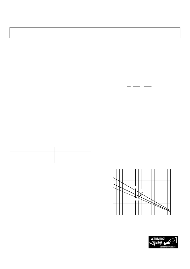
Figure 5 shows the maximum safe power dissipation in the
package vs. the ambient temperature for the 8-lead MSOP
(145°C/W), 8-lead SOIC_N (125°C/W) and the 6-lead SOT-23
(170°C/W) on a JEDEC standard 4-layer board. θ
JA
values are
approximations.
2.0
0
–55
125
0
AMBIENT TEMPERATURE (°C)
M
1.5
1.0
0.5
–45 –35 –25 –15 –5
5
15 25 35 45 55 65 75 85 95 105 115
SOT-23
SOIC
MSOP
Figure 5. Maximum Power Dissipation vs. Temperature for a 4-Layer Board
ESD CAUTION
ESD (electrostatic discharge) sensitive device. Electrostatic charges as high as 4000 V readily accumulate on
the human body and test equipment and can discharge without detection. Although this product features
proprietary ESD protection circuitry, permanent damage may occur on devices subjected to high energy
electrostatic discharges. Therefore, proper ESD precautions are recommended to avoid performance
degradation or loss of functionality.
相關PDF資料 |
PDF描述 |
|---|---|
| ADA4841-2YRZ-R7 | Low Power, Low Noise and Distortion, Rail-to-Rail Output Amplifier |
| ADA4841-2YRZ-RL | Low Power, Low Noise and Distortion, Rail-to-Rail Output Amplifier |
| ADA4841-X | 16-Bit, 8-Channel, 250 kSPS PulSAR㈢ ADC. |
| AD7682 | 16-Bit, 8-Channel, 250 kSPS PulSAR㈢ ADC. |
| AD7689 | 16-Bit, 8-Channel, 250 kSPS PulSAR㈢ ADC. |
相關代理商/技術參數 |
參數描述 |
|---|---|
| ADA4841-2YRZ-R7 | 功能描述:IC OPAMP VF R-R DUAL LP LN 8SOIC RoHS:是 類別:集成電路 (IC) >> Linear - Amplifiers - Instrumentation 系列:- 標準包裝:100 系列:- 放大器類型:通用 電路數:1 輸出類型:- 轉換速率:0.2 V/µs 增益帶寬積:- -3db帶寬:- 電流 - 輸入偏壓:100pA 電壓 - 輸入偏移:30µV 電流 - 電源:380µA 電流 - 輸出 / 通道:- 電壓 - 電源,單路/雙路(±):±2 V ~ 18 V 工作溫度:0°C ~ 70°C 安裝類型:表面貼裝 封裝/外殼:8-SOIC(0.154",3.90mm 寬) 供應商設備封裝:8-SO 包裝:管件 |
| ADA4841-2YRZ-RL | 功能描述:IC OPAMP VF R-R DUAL LP LN 8SOIC RoHS:是 類別:集成電路 (IC) >> Linear - Amplifiers - Instrumentation 系列:- 產品培訓模塊:Lead (SnPb) Finish for COTS Obsolescence Mitigation Program 標準包裝:1 系列:- 放大器類型:電流檢測 電路數:1 輸出類型:- 轉換速率:- 增益帶寬積:125kHz -3db帶寬:- 電流 - 輸入偏壓:- 電壓 - 輸入偏移:100µV 電流 - 電源:1.1µA 電流 - 輸出 / 通道:- 電壓 - 電源,單路/雙路(±):- 工作溫度:-40°C ~ 85°C 安裝類型:表面貼裝 封裝/外殼:4-WFBGA,CSPBGA 供應商設備封裝:4-UCSP(2x2) 包裝:剪切帶 (CT) 其它名稱:MAX9634WERS+TCT |
| ADA4841-X | 制造商:AD 制造商全稱:Analog Devices 功能描述:14-Bit, 8-Channel, 250 kSPS PulSAR ADC |
| ADA4850-1 | 制造商:AD 制造商全稱:Analog Devices 功能描述:High Speed, Rail-to-Rail Output Op Amps with Ultralow Power-Down |
| ADA4850-1_07 | 制造商:AD 制造商全稱:Analog Devices 功能描述:High Speed, Rail-to-Rail Output Op Amps with Ultralow Power-Down |
發布緊急采購,3分鐘左右您將得到回復。