- 您現在的位置:買賣IC網 > PDF目錄373975 > ADAU1401YSTZ-RL (ANALOG DEVICES INC) SigmaDSP 28-/56-Bit Audio Processor with Two ADCs and Four DACs PDF資料下載
參數資料
| 型號: | ADAU1401YSTZ-RL |
| 廠商: | ANALOG DEVICES INC |
| 元件分類: | 消費家電 |
| 英文描述: | SigmaDSP 28-/56-Bit Audio Processor with Two ADCs and Four DACs |
| 中文描述: | SPECIALTY CONSUMER CIRCUIT, PQFP48 |
| 封裝: | ROHS COMPLIANT, PLASTIC, MS-026BBC, LQFP-48 |
| 文件頁數: | 17/52頁 |
| 文件大小: | 785K |
| 代理商: | ADAU1401YSTZ-RL |
第1頁第2頁第3頁第4頁第5頁第6頁第7頁第8頁第9頁第10頁第11頁第12頁第13頁第14頁第15頁第16頁當前第17頁第18頁第19頁第20頁第21頁第22頁第23頁第24頁第25頁第26頁第27頁第28頁第29頁第30頁第31頁第32頁第33頁第34頁第35頁第36頁第37頁第38頁第39頁第40頁第41頁第42頁第43頁第44頁第45頁第46頁第47頁第48頁第49頁第50頁第51頁第52頁
ADAU1401
ADCs, and each DAC can be powered down individually. The
current savings is about 15 mA when the ADCs are powered
down and about 4 mA for each DAC that is powered down. The
voltage reference, which is supplied to both the ADCs and
DACs, should only be powered down if all ADCs and DACs are
powered down. The reference is powered down by setting both
Bit 6 and Bit 7 of the control register.
USING THE OSCILLATOR
The ADAU1401 can use an on-board oscillator to generate its
master clock. The oscillator is designed to work with a 256 × f
S
master clock, which is 12.288 MHz for a f
S
of 48 kHz and
11.2896 MHz for a f
S
of 44.1 kHz. The crystal in the oscillator
circuit should be an AT-cut, parallel resonator operating at its
fundamental frequency.
Figure 14 shows the external circuit
recommended for proper operation.
ADAU1401
Rev. 0 | Page 17 of 52
If the oscillator is not utilized in the design, it can be powered
down to save power. This can be done if a system master clock
is already available in the system. By default, the oscillator is
powered on. The oscillator powers down when a 1 is written to
the OPD bit of the oscillator power-down register (see Table 61).
SETTING MASTER CLOCK/PLL MODE
The MCLKI input of the ADAU1401 feeds a PLL, which generates
the 50 MIPS SigmaDSP core clock. In normal operation, the
input to MCLKI must be one of the following: 64 × f
S
, 256 × f
S
,
384 × f
S
, or 512 × f
S
, where f
S
is the input sampling rate. The
mode is set on PLL_MODE0 and PLL_MODE1 as described in
Table 13. If the ADAU1401 is set to receive double-rate signals
(by reducing the number of program steps per sample by a factor
of 2 using the core control register), the master clock frequency
must be 32 × f
S
, 128 × f
S
, 192 × f
S
, or 256 × f
S
. If the ADAU1401
is set to receive quad-rate signals (by reducing the number of
program steps per sample by a factor of 4 using the core control
register), the master clock frequency must be 16 × f
S
, 64 × f
S
, 96 × f
S
,
or 128 × f
S
. On power-up, a clock signal must be present on
MCLK so that the ADAU1401 can complete its initialization
routine.
C1
100
MCLKI
OSCO
C2
0
Figure 14. Crystal Oscillator Circuit
Table 13. PLL Modes
MCLKI Input
64 × f
S
256 × f
S
384 × f
S
512 × f
S
The clock mode should not be changed without also resetting
the ADAU1401. If the mode is changed during operation, a
click or pop can result in the output signals. The state of the
PLL_MODEx pins should be changed while
The 100 Ω damping resistor on OSCO gives the oscillator a
voltage swing of approximately 2.2 V. The crystal shunt capaci-
tance should be 7 pF. Its load capacitance should be about 18 pF,
although the circuit supports values of up to 25 pF. The necessary
values of the C1 and C2 load capacitors can be calculated from
the crystal load capacitance as follows:
C2
C1
C
+
+
where
C
stray
is the stray capacitance in the circuit and is usually
assumed to be approximately 2 pF to 5 pF.
OSCO should not be used to directly drive the crystal signal to
another IC. This signal is an analog sine wave, and it is not appro-
priate to use it to drive a digital input. There are two options for
using the ADAU1401 to provide a master clock to other ICs in
the system. The first, and less recommended, method is to use a
high impedance input digital buffer on the OSCO signal. If this
is done, minimize the trace length to the buffer input. The second
method is to use a clock from the serial output port. Pin MP11 can
be set as an output (master) clock divided down from the internal
core clock. If this pin is set to serial output port (OUTPUT_BCLK)
mode in the multipurpose pin configuration register (2081) and
the port is set to master in the serial output control register (2078),
the desired output frequency can also be set in the serial output
control register with Bits OBF [1:0] (see Table 50).
PLL_MODE0
0
0
1
1
PLL_MODE1
0
1
0
1
stray
L
C
C2
C1
×
=
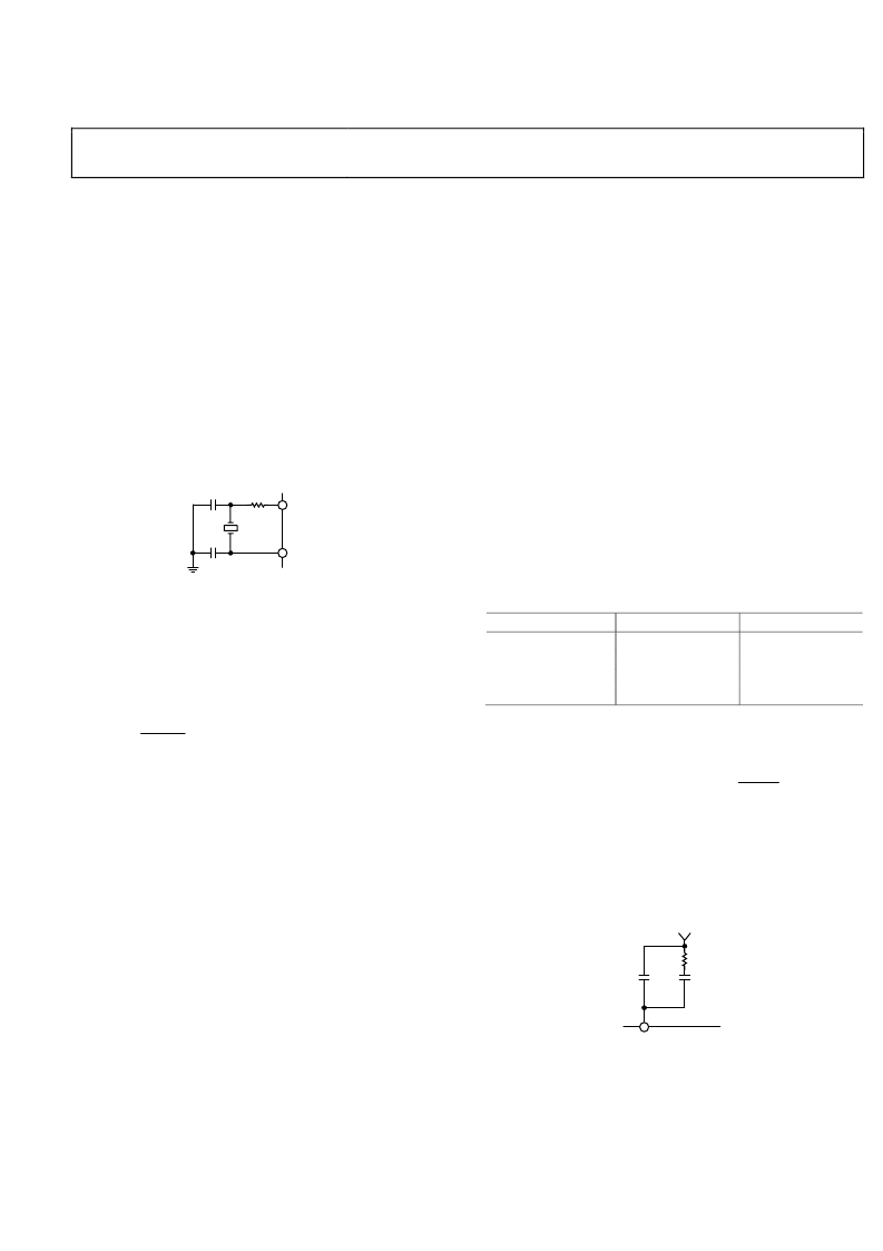
RESET is held low.
The PLL loop filter should be connected to the PLL_LF pin. This
filter, shown in Figure 15, includes three passive components—
two capacitors and a resistor. The values of these components
do not need to be exact; the tolerance can be up to 10% for the
resistor and up to 20% for the capacitors. The 3.3 V signal shown in
Figure 15 can be connected to the AVDD supply of the chip.
ADAU1401
3.3V
475
PLL_LF
56nF
3.3nF
0
Figure 15. PLL Loop Filter
相關PDF資料 |
PDF描述 |
|---|---|
| ADAU1513 | Class-D Audio Power Stage |
| ADAU1513ACPZ | Class-D Audio Power Stage |
| ADAU1513ACPZ-RL | Class-D Audio Power Stage |
| ADAU1513ACPZ-RL7 | Class-D Audio Power Stage |
| ADAU1513ASVZ | Class-D Audio Power Stage |
相關代理商/技術參數 |
參數描述 |
|---|---|
| ADAU1421YSTZ | 制造商:Analog Devices 功能描述: |
| ADAU1421YSTZ-REEL | 制造商:Analog Devices 功能描述: |
| ADAU1442 | 制造商:AD 制造商全稱:Analog Devices 功能描述:SigmaDSP Digital Audio Processor |
| ADAU1442YSVZ-3A | 功能描述:IC SIGMADSP 28B 175MHZ 100TQFP RoHS:是 類別:集成電路 (IC) >> 線性 - 音頻處理 系列:SigmaDSP® 其它有關文件:STA321 View All Specifications 標準包裝:1 系列:Sound Terminal™ 類型:音頻處理器 應用:數字音頻 安裝類型:表面貼裝 封裝/外殼:64-LQFP 裸露焊盤 供應商設備封裝:64-LQFP EP(10x10) 包裝:Digi-Reel® 其它名稱:497-11050-6 |
| ADAU1442YSVZ-3A-RL | 功能描述:IC SIGMADSP 28B 175MHZ 100TQFP RoHS:是 類別:集成電路 (IC) >> 線性 - 音頻處理 系列:SigmaDSP® 其它有關文件:STA321 View All Specifications 標準包裝:1 系列:Sound Terminal™ 類型:音頻處理器 應用:數字音頻 安裝類型:表面貼裝 封裝/外殼:64-LQFP 裸露焊盤 供應商設備封裝:64-LQFP EP(10x10) 包裝:Digi-Reel® 其它名稱:497-11050-6 |
發布緊急采購,3分鐘左右您將得到回復。