- 您現在的位置:買賣IC網 > PDF目錄373982 > ADF4113HVBRUZ (ANALOG DEVICES INC) High Voltage Charge Pump, PLL Synthesizer PDF資料下載
參數資料
| 型號: | ADF4113HVBRUZ |
| 廠商: | ANALOG DEVICES INC |
| 元件分類: | XO, clock |
| 英文描述: | High Voltage Charge Pump, PLL Synthesizer |
| 中文描述: | PLL FREQUENCY SYNTHESIZER, 3700 MHz, PDSO16 |
| 封裝: | LEAD FREE, MO-153AB, TSSOP-16 |
| 文件頁數: | 16/20頁 |
| 文件大小: | 385K |
| 代理商: | ADF4113HVBRUZ |
ADF4113HV
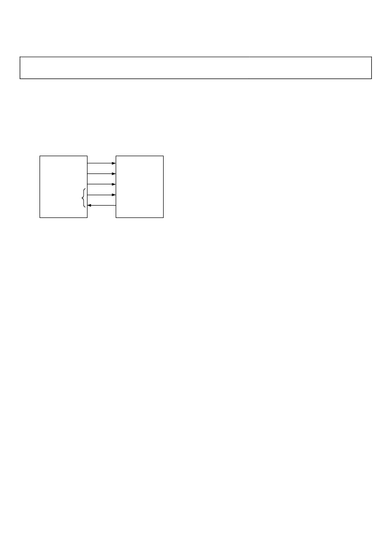
ADSP-21xx Interface
Figure 25 shows the interface between the ADF4113HV and the
ADSP-21xx digital signal processor. The ADF4113HV needs a
24-bit serial word for each latch write. The easiest way to
accomplish this using the ADSP-21xx family is to use the auto
buffered transmit mode of operation with alternate framing.
This provides a means for transmitting an entire block of serial
data before an interrupt is generated.
Rev. 0 | Page 16 of 20
SCLK
DT
I/O FLAGS
ADSP-21xx
CLK
DATA
LE
CE
MUXOUT
(LOCK DETECT)
ADF4113HV
TFS
0
Figure 25. ADSP-21xx to ADF4113HV Interface
Set up the word length for eight bits and use three memory
locations for each 24-bit word. To program each 24-bit latch,
store the three 8-bit bytes, enable the auto buffered mode, and
then write to the transmit register of the DSP. This last opera-
tion initiates the autobuffer transfer.
PCB DESIGN GUIDELINES FOR CHIP SCALE
PACKAGE
The lands on the chip scale package (CP-20-1) are rectangular.
The printed circuit board pad for these should be 0.1 mm
longer than the package land length, and 0.05 mm wider than
the package land width. The land should be centered on the pad
to ensure that the solder joint size is maximized.
The bottom of the chip scale package has a central thermal pad.
The thermal pad on the printed circuit board should be at least
as large as this exposed pad. On the printed circuit board, provide
a clearance of at least 0.25 mm between the thermal pad and the
inner edges of the pad pattern. This ensures that shorting is
avoided.
Thermal vias can be used on the printed circuit board thermal
pad to improve thermal performance of the package. If vias are
used, they should be incorporated in the thermal pad at a 1.2 mm
pitch grid. The via diameter should be between 0.3 mm and
0.33 mm, and the via barrel should be plated with 1 oz. copper
to plug the via.
The user should connect the printed circuit board thermal pad
to AGND.
相關PDF資料 |
PDF描述 |
|---|---|
| ADF4113HVBRUZ-RL | High Voltage Charge Pump, PLL Synthesizer |
| ADF4113HVBRUZ-RL7 | High Voltage Charge Pump, PLL Synthesizer |
| ADF4116 | PLL Frequency Synthesizer(PLL頻率合成器) |
| ADF4118 | RF PLL Frequency Synthesizers |
| ADF4117BCP | BATT LITHIUM COIN 3V 48MAH COIN-W/LEGS 12.5MM |
相關代理商/技術參數 |
參數描述 |
|---|---|
| ADF4113HVBRUZ-RL | 功能描述:IC CHARGE PUMP HV SYNTH 16-TSSOP RoHS:是 類別:集成電路 (IC) >> 時鐘/計時 - 時鐘發生器,PLL,頻率合成器 系列:- 標準包裝:1,000 系列:Precision Edge® 類型:時鐘/頻率合成器 PLL:無 輸入:CML,PECL 輸出:CML 電路數:1 比率 - 輸入:輸出:2:1 差分 - 輸入:輸出:是/是 頻率 - 最大:10.7GHz 除法器/乘法器:無/無 電源電壓:2.375 V ~ 3.6 V 工作溫度:-40°C ~ 85°C 安裝類型:表面貼裝 封裝/外殼:16-VFQFN 裸露焊盤,16-MLF? 供應商設備封裝:16-MLF?(3x3) 包裝:帶卷 (TR) 其它名稱:SY58052UMGTRSY58052UMGTR-ND |
| ADF4113HVBRUZ-RL7 | 功能描述:IC CHARGE PUMP HV SYNTH 16-TSSOP RoHS:是 類別:集成電路 (IC) >> 時鐘/計時 - 時鐘發生器,PLL,頻率合成器 系列:- 標準包裝:1,000 系列:Precision Edge® 類型:時鐘/頻率合成器 PLL:無 輸入:CML,PECL 輸出:CML 電路數:1 比率 - 輸入:輸出:2:1 差分 - 輸入:輸出:是/是 頻率 - 最大:10.7GHz 除法器/乘法器:無/無 電源電壓:2.375 V ~ 3.6 V 工作溫度:-40°C ~ 85°C 安裝類型:表面貼裝 封裝/外殼:16-VFQFN 裸露焊盤,16-MLF? 供應商設備封裝:16-MLF?(3x3) 包裝:帶卷 (TR) 其它名稱:SY58052UMGTRSY58052UMGTR-ND |
| ADF4113HVSD1Z | 制造商:Analog Devices 功能描述:- Rail/Tube |
| ADF4116 | 制造商:AD 制造商全稱:Analog Devices 功能描述:RF PLL Frequency Synthesizers |
| ADF4116_07 | 制造商:AD 制造商全稱:Analog Devices 功能描述:RF PLL Frequency Synthesizers |
發布緊急采購,3分鐘左右您將得到回復。