- 您現(xiàn)在的位置:買賣IC網(wǎng) > PDF目錄373982 > ADF4208BRU (ANALOG DEVICES INC) Dual RF PLL Frequency Synthesizers PDF資料下載
參數(shù)資料
| 型號: | ADF4208BRU |
| 廠商: | ANALOG DEVICES INC |
| 元件分類: | XO, clock |
| 英文描述: | Dual RF PLL Frequency Synthesizers |
| 中文描述: | PLL FREQUENCY SYNTHESIZER, 2000 MHz, PDSO20 |
| 封裝: | TSSOP-20 |
| 文件頁數(shù): | 5/20頁 |
| 文件大小: | 206K |
| 代理商: | ADF4208BRU |
REV. 0
ADF4206/ADF4207/ADF4208
–5–
PIN FUNCTION DESCRIPTIONS
Mnemonic
Pin
No.
ADF4206/
ADF4207
ADF4208
Function
Positive Power Supply for the RF1 Section. A 0.1
μ
F capacitor should be connected between
this pin and the RF1 ground pin, DGND
RF1
. V
DD
1 should have a value of between 2.7 V and
5.5 V. V
DD
1 must have the same potential as V
DD
2.
Power Supply for the RF1 Charge Pump. This should be greater than or equal to V
DD
.
Output from the RF1 Charge Pump. This is normally connected to a loop filter which, in
turn, drives the input to an external VCO.
Ground Pin for the RF1 Digital Circuitry.
Input to the RF1 Prescaler. This low-level input signal is normally taken from the RF1 VCO.
Complementary Input to the RF1 Prescaler of the ADF4208. This point should be decoupled to
the ground plane with a small bypass capacitor.
Ground Pin for the RF1 Analog Circuitry.
Oscillator Input. It has a V
DD
/2 threshold and can be driven from an external CMOS or TTL
logic gate.
Oscillator Output.
This multiplexer output allows either the IF/RF lock detect, the scaled RF, or the scaled
Reference Frequency to be accessed externally. See Table V.
Serial Clock Input. This serial clock is used to clock in the serial data to the registers. The
data is latched into the 22-bit shift register on the CLK rising edge. This input is a high
impedance CMOS input.
Serial Data Input. The serial data is loaded MSB first with the two LSBs being the control
bits. This input is a high impedance CMOS input.
Load Enable, CMOS Input. When LE goes high, the data stored in the shift registers is
loaded into one of the four latches, the latch being selected using the control bits.
Ground Pin for the RF2 Analog Circuitry.
Complementary Input to the RF2 Prescaler. This point should be decoupled to the ground
plane with a small bypass capacitor.
Input to the RF2 Prescaler. This low-level input signal is normally ac-coupled to the
external VCO.
Ground Pin for the RF2, Digital, Interface, and Control Circuitry.
Output from the RF2 Charge Pump. This is normally connected to a loop filter that drives
the input to an external VCO.
Power Supply for the RF2 Charge Pump. This should be greater than or equal to V
DD
.
Positive Power Supply for the RF2, Interface, and Oscillator Sections. A 0.1
μ
F capacitor
should be connected between this pin and the RF2 ground Pin, DGND
RF2
. V
DD
2 should
have a value between 2.7 V and 5.5 V. V
DD
2 must have the same potential as V
DD
1.
1
V
DD
1
V
DD
1
2
3
V
P
1
CP
RF1
V
P
1
CP
RF1
4
5
6
DGND
RF1
RF1
IN
OSC
IN
DGND
RF1
RF1
IN
A
RF
IN
B
7
8
OSC
OUT
MUXOUT
AGND
RF1
OSC
IN
9
10
CLK
DATA
OSC
OUT
MUXOUT
11
LE
CLK
12
RF2
IN
DATA
13
DGND
RF2
LE
14
15
CP
RF2
V
P
2
AGND
RF2
RF2
IN
B
16
V
DD
2
RF2
IN
A
17
18
DGND
RF2
CP
RF2
19
20
V
P
2
V
DD
2
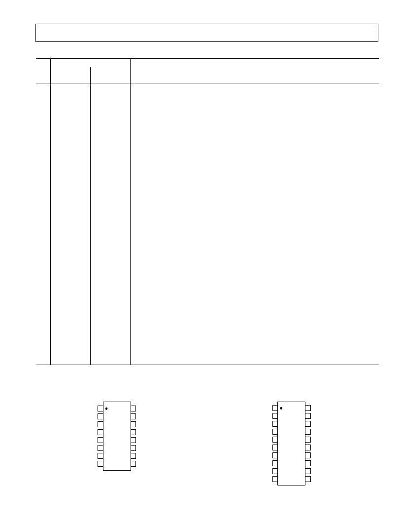
PIN CONFIGURATIONS
TSSOP
TOP VIEW
(Not to Scale)
16
15
14
13
12
11
10
9
1
2
3
4
5
6
7
8
V
DD
1
V
P
1
CP
RF1
DGND
RF1
RF1
IN
OSC
IN
OSC
OUT
MUXOUT
V
DD
2
V
P
2
CP
RF2
DGND
RF2
RF2
IN
LE
DATA
CLK
ADF4206/
ADF4207
TSSOP
TOP VIEW
(Not to Scale)
20
19
18
17
16
15
14
13
12
11
1
2
3
4
5
6
7
8
9
10
ADF4208
V
DD
1
V
P
1
CP
RF1
DGND
RF1
RF1
IN
A
OSC
IN
OSC
OUT
MUXOUT
V
DD
2
V
P
2
CP
RF2
AGND
RF2
LE
DATA
CLK
RF1
IN
B
AGND
RF1
RF2
IN
B
RF2
IN
A
DGND
RF2
相關(guān)PDF資料 |
PDF描述 |
|---|---|
| ADF4206 | Dual RF PLL Frequency Synthesizers |
| ADF4206BRU | Dual RF PLL Frequency Synthesizers |
| ADF4212 | Dual RF/IF PLL Frequency Synthesizers |
| ADF4210 | Dual RF/IF PLL Frequency Synthesizers |
| ADF4210BCP | Dual RF/IF PLL Frequency Synthesizers |
相關(guān)代理商/技術(shù)參數(shù) |
參數(shù)描述 |
|---|---|
| ADF4208BRU-REEL | 制造商:Analog Devices 功能描述:PLL Frequency Synthesizer Dual 20-Pin TSSOP T/R |
| ADF4208BRU-REEL7 | 制造商:Analog Devices 功能描述:PLL Frequency Synthesizer Dual 20-Pin TSSOP T/R |
| ADF4208BRUZ | 功能描述:IC PLL FREQ SYNTHESIZER 20TSSOP RoHS:是 類別:集成電路 (IC) >> 時(shí)鐘/計(jì)時(shí) - 時(shí)鐘發(fā)生器,PLL,頻率合成器 系列:- 標(biāo)準(zhǔn)包裝:1,000 系列:Precision Edge® 類型:時(shí)鐘/頻率合成器 PLL:無 輸入:CML,PECL 輸出:CML 電路數(shù):1 比率 - 輸入:輸出:2:1 差分 - 輸入:輸出:是/是 頻率 - 最大:10.7GHz 除法器/乘法器:無/無 電源電壓:2.375 V ~ 3.6 V 工作溫度:-40°C ~ 85°C 安裝類型:表面貼裝 封裝/外殼:16-VFQFN 裸露焊盤,16-MLF? 供應(yīng)商設(shè)備封裝:16-MLF?(3x3) 包裝:帶卷 (TR) 其它名稱:SY58052UMGTRSY58052UMGTR-ND |
| ADF4208BRUZ-R7 | 功能描述:IC PLL FREQ SYNTHESIZER 20TSSOP RoHS:是 類別:集成電路 (IC) >> 時(shí)鐘/計(jì)時(shí) - 時(shí)鐘發(fā)生器,PLL,頻率合成器 系列:- 標(biāo)準(zhǔn)包裝:1,000 系列:Precision Edge® 類型:時(shí)鐘/頻率合成器 PLL:無 輸入:CML,PECL 輸出:CML 電路數(shù):1 比率 - 輸入:輸出:2:1 差分 - 輸入:輸出:是/是 頻率 - 最大:10.7GHz 除法器/乘法器:無/無 電源電壓:2.375 V ~ 3.6 V 工作溫度:-40°C ~ 85°C 安裝類型:表面貼裝 封裝/外殼:16-VFQFN 裸露焊盤,16-MLF? 供應(yīng)商設(shè)備封裝:16-MLF?(3x3) 包裝:帶卷 (TR) 其它名稱:SY58052UMGTRSY58052UMGTR-ND |
| ADF4208BRUZ-RL | 功能描述:IC PLL FREQ SYNTHESIZER 20TSSOP RoHS:是 類別:集成電路 (IC) >> 時(shí)鐘/計(jì)時(shí) - 時(shí)鐘發(fā)生器,PLL,頻率合成器 系列:- 標(biāo)準(zhǔn)包裝:1,000 系列:Precision Edge® 類型:時(shí)鐘/頻率合成器 PLL:無 輸入:CML,PECL 輸出:CML 電路數(shù):1 比率 - 輸入:輸出:2:1 差分 - 輸入:輸出:是/是 頻率 - 最大:10.7GHz 除法器/乘法器:無/無 電源電壓:2.375 V ~ 3.6 V 工作溫度:-40°C ~ 85°C 安裝類型:表面貼裝 封裝/外殼:16-VFQFN 裸露焊盤,16-MLF? 供應(yīng)商設(shè)備封裝:16-MLF?(3x3) 包裝:帶卷 (TR) 其它名稱:SY58052UMGTRSY58052UMGTR-ND |
發(fā)布緊急采購,3分鐘左右您將得到回復(fù)。