- 您現在的位置:買賣IC網 > PDF目錄373983 > ADF4360-8BCPRL (ANALOG DEVICES INC) Integrated Synthesizer and VCO PDF資料下載
參數資料
| 型號: | ADF4360-8BCPRL |
| 廠商: | ANALOG DEVICES INC |
| 元件分類: | 無繩電話/電話 |
| 英文描述: | Integrated Synthesizer and VCO |
| 中文描述: | TELECOM, CELLULAR, BASEBAND CIRCUIT, QCC24 |
| 封裝: | 4 X 4 MM, MO-220-VGGD-2, LFCSP-24 |
| 文件頁數: | 10/24頁 |
| 文件大小: | 539K |
| 代理商: | ADF4360-8BCPRL |
ADF4360-5
MUXOUT AND LOCK DETECT
The output multiplexer on the ADF4360 family allows the user
to access various internal points on the chip. The state of
MUXOUT is controlled by M3, M2, and M1 in the function
latch. The full truth table is shown in Table 7. Figure 13 shows
the MUXOUT section in block diagram form.
Lock Detect
MUXOUT can be programmed for two types of lock detect:
digital and analog. Digital lock detect is active high. When LDP
in the R counter latch is set to 0, digital lock detect is set high
when the phase error on three consecutive phase detector cycles
is less than 15 ns.
Rev. 0 | Page 10 of 24
With LDP set to 1, five consecutive cycles of less than 15 ns
phase error are required to set the lock detect. It stays set high
until a phase error of greater than 25 ns is detected on any sub-
sequent PD cycle.
The N-channel open-drain analog lock detect should be oper-
ated with an external pull-up resistor of 10 k nominal. When a
lock has been detected, this output is high with narrow low-
going pulses.
R COUNTER OUTPUT
N COUNTER OUTPUT
DIGITAL LOCK DETECT
DGND
CONTROL
MUX
MUXOUT
DV
DD
ANALOG LOCK DETECT
SDOUT
0
Figure 13. MUXOUT Circuit
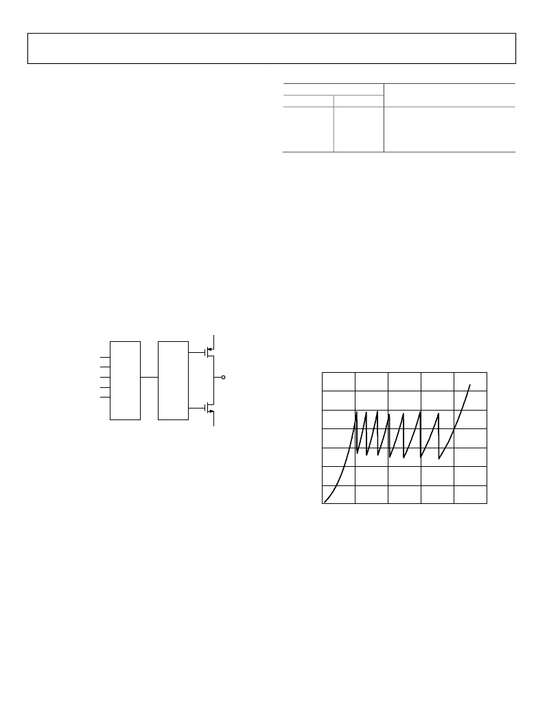
INPUT SHIFT REGISTER
The ADF4360 family’s digital section includes a 24-bit input
shift register, a 14-bit R counter, and an 18-bit N counter,
comprised of a 5-bit A counter and a 13-bit B counter. Data is
clocked into the 24-bit shift register on each rising edge of CLK.
The data is clocked in MSB first. Data is transferred from the
shift register to one of four latches on the rising edge of LE. The
destination latch is determined by the state of the two control
bits (C2, C1) in the shift register. The two LSBs are DB1 and
DB0, as shown in Figure 2.
The truth table for these bits is shown in Table 5. Table 6 shows
a summary of how the latches are programmed. Note that the
test modes latch is used for factory testing and should not be
programmed by the user.
Table 5. C2 and C1 Truth Table
Control Bits
C2
C1
0
0
0
1
1
0
1
1
VCO
The VCO core in the ADF4360 family uses eight overlapping
bands, as shown in Figure 14, to allow a wide frequency range to
be covered without a large VCO sensitivity (K
V
) and resultant
poor phase noise and spurious performance.
Data Latch
Control Latch
R Counter
N Counter (A and B)
Test Modes Latch
The correct band is chosen automatically by the band select
logic at power-up or whenever the N counter latch is updated. It
is important that the correct write sequence be followed at
power-up. This sequence is
1.
2.
3.
R counter latch
Control latch
N counter latch
During band selection, which takes five PFD cycles, the VCO
V
TUNE
is disconnected from the output of the loop filter and is
connected to an internal reference voltage.
0
900
0.5
1.0
1.5
2.0
2.5
3.0
3.5
1000
1100
FREQUENCY (MHz)
1200
1300
1400
V
0
Figure 14. Frequency vs. V
TUNE
, ADF4360-5
The R counter output is used as the clock for the band select logic
and should not exceed 1 MHz. A programmable divider is provided
at the R counter input to allow division by 1, 2, 4, or 8 and is con-
trolled by Bits BSC1 and BSC2 in the R counter latch. Where the
required PFD frequency exceeds 1 MHz, the divide ratio should be
set to allow enough time for correct band selection.
After band select, normal PLL action resumes. The nominal value
of K
V
is 31 MHz/V or 15 MHz/V if divide-by-2 operation has been
selected (by programming DIV2 (DB22) high in the N counter
latch). The ADF4360 family contains linearization circuitry to
minimize any variation of the product of I
CP
and K
V
.
相關PDF資料 |
PDF描述 |
|---|---|
| ADF4360-8BCPRL7 | Integrated Synthesizer and VCO |
| ADF4360-1 | Integrated Synthesizer and VCO |
| ADF4360-1BCPRL | Integrated Synthesizer and VCO |
| ADF7010BRU | High Performance ISM Band ASK/FSK/GFSK Transmitter IC |
| ADF7010 | High Performance ISM Band ASK/FSK/GFSK Transmitter IC |
相關代理商/技術參數 |
參數描述 |
|---|---|
| ADF4360-8BCPRL7 | 制造商:Analog Devices 功能描述:Integrated Synthesizer 24-Pin LFCSP EP T/R |
| ADF4360-8BCPZ | 功能描述:IC SYNTHESIZER VCO 24-LFCSP RoHS:是 類別:集成電路 (IC) >> 時鐘/計時 - 時鐘發生器,PLL,頻率合成器 系列:- 標準包裝:2,000 系列:- 類型:PLL 頻率合成器 PLL:是 輸入:晶體 輸出:時鐘 電路數:1 比率 - 輸入:輸出:1:1 差分 - 輸入:輸出:無/無 頻率 - 最大:1GHz 除法器/乘法器:是/無 電源電壓:4.5 V ~ 5.5 V 工作溫度:-20°C ~ 85°C 安裝類型:表面貼裝 封裝/外殼:16-LSSOP(0.175",4.40mm 寬) 供應商設備封裝:16-SSOP 包裝:帶卷 (TR) 其它名稱:NJW1504V-TE1-NDNJW1504V-TE1TR |
| ADF4360-8BCPZ | 制造商:Analog Devices 功能描述:PLL/Frequency Synthesizer IC |
| ADF4360-8BCPZ1 | 制造商:AD 制造商全稱:Analog Devices 功能描述:Integrated Synthesizer and VCO |
| ADF4360-8BCPZRL | 功能描述:IC SYNTHESIZER VCO 24LFCSP RoHS:是 類別:集成電路 (IC) >> 時鐘/計時 - 時鐘發生器,PLL,頻率合成器 系列:- 標準包裝:1,000 系列:Precision Edge® 類型:時鐘/頻率合成器 PLL:無 輸入:CML,PECL 輸出:CML 電路數:1 比率 - 輸入:輸出:2:1 差分 - 輸入:輸出:是/是 頻率 - 最大:10.7GHz 除法器/乘法器:無/無 電源電壓:2.375 V ~ 3.6 V 工作溫度:-40°C ~ 85°C 安裝類型:表面貼裝 封裝/外殼:16-VFQFN 裸露焊盤,16-MLF? 供應商設備封裝:16-MLF?(3x3) 包裝:帶卷 (TR) 其它名稱:SY58052UMGTRSY58052UMGTR-ND |
發布緊急采購,3分鐘左右您將得到回復。