- 您現在的位置:買賣IC網 > PDF目錄373983 > ADF7011 (Analog Devices, Inc.) High Performance ISM Band ASK/FSK/GFSK Transmitter IC PDF資料下載
參數資料
| 型號: | ADF7011 |
| 廠商: | Analog Devices, Inc. |
| 元件分類: | 調制器/解調器 |
| 英文描述: | High Performance ISM Band ASK/FSK/GFSK Transmitter IC |
| 中文描述: | 高性能ISM頻段詢價/ FSK信號/發射器集成電路的GFSK |
| 文件頁數: | 15/24頁 |
| 文件大小: | 567K |
| 代理商: | ADF7011 |
REV. 0
ADF7011
–15–
CIRCUIT DESCRIPTION
Reference Input Section
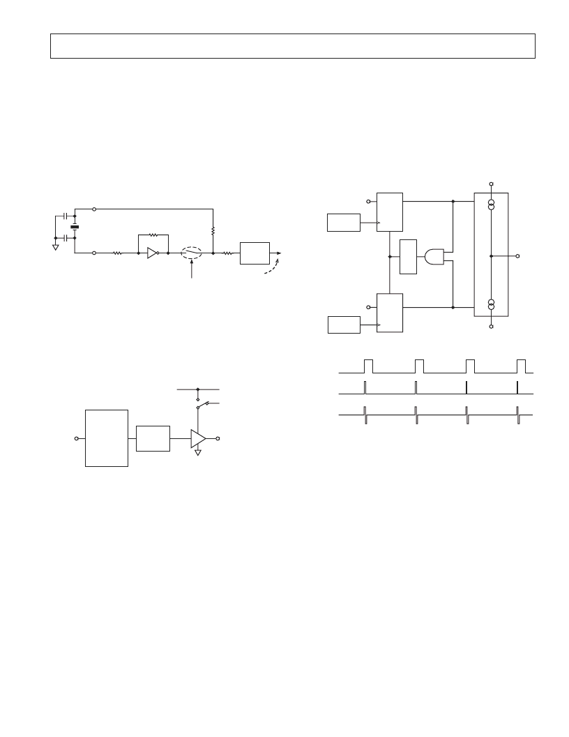
The on-board crystal oscillator circuitry (Figure 2), allows the
use of an inexpensive quartz crystal as the PLL reference. The
oscillator circuit is enabled by setting
XOE
low. It is enabled by
default on power-up and is disabled by bringing CE low. Two
parallel resonant capacitors are required for oscillation at the
correct frequency; the value of these is dependant on the crystal
specification. Errors in the crystal can be corrected using the
error correction register within the R register. A single-ended
reference (TCXO, CXO) may be used. The CMOS levels should
be applied to OSC2, with
XOE
set high.
TO R COUNTER AND
CLK
OUT
DIVIDE
BUFFER
SW1
100k
10pF
OSC2
NC
XTAL OSCILLATOR
DISABLED
10pF
OSC1
500k
100k
Figure 2. Oscillator Circuit on the ADF7011
CLK
OUT
Divider and Buffer
The CLK
OUT
circuit takes the reference clock signal from the
oscillator section above and supplies a divided down 50:50 mark-
space signal to the CLK
OUT
pin. An even divide from 2 to 30 is
available. This divide is set by the four MSBs in the R register.
On power-up, the CLK
OUT
defaults to divide by 16.
CLK
OUT
DV
DD
OSC1
DIVIDER
1 TO 15
DIVIDE
BY 2
CLK
OUT
ENABLE BIT
Figure 3. CLK
OUT
Stage
The output buffer to CLK
OUT
is enabled by setting Bit DB4 in
the function register high. On power-up, this bit is set high.
The output buffer can drive up to a 20 pF load with a 10% rise
time at 4.8 MHz. Faster edges can result in some spurious
feedthrough to the output. A small series resistor (50
) can be
used to slow the clock edges to reduce these spurs at F
CLK
.
R Counter
The 4-bit R Counter divides the reference input frequency by
an integer from 1 to 15. The divided down signal is presented
as the reference clock to the phase frequency detector (PFD).
The divide ratio is set in the R register. Maximizing the PFD
frequency reduces the N value. Having a higher PFD will
result in a higher level of spurious components. A PFD of
close to 4 MHz is recommended. This reduces the noise multi-
plied at a rate of 20 log(N) to the output, as well as reduces
occurrences of spurious components. The R register defaults
to R = 1 on power-up.
Prescaler, Phase Frequency Detector (PFD), and
Charge Pump
The dual-modulus prescaler (
P/P
+ 1) divides the RF signal
from the VCO to a lower frequency that is manageable by the
CMOS counters.
The PFD takes inputs from the R Counter and the N Counter
(
N
=
Int
+
Fraction
) and produces an output proportional to the
phase and frequency difference between them. Figure 4 is a
simplified schematic.
CP
D
E
U3
UP
CHARGE
PUMP
CP
GND
V
P
N DIVIDER
HI
D2
Q2
CLR2
U2
DOWN
HI
D1
Q1
CLR1
U1
R DIVIDER
R DIVIDER
N DIVIDER
CP OUTPUT
Figure 4. PFD Stage
The PFD includes a delay element that sets the width of the
antibacklash pulse. The typical value for this in the ADF7011 is
3 ns. This pulse ensures that there is no dead zone in the PFD
transfer function and minimizes phase noise and reference spurs.
MUXOUT and Lock Detect
The MUXOUT pin allows the user to access various internal
points in the ADF7011. The state of MUXOUT is controlled
by Bits M1 to M4 in the function register.
Regulator Ready
This is the default setting on MUXOUT after the transmitter
has been powered up. The power-up time of the regulator is
typically 50
μ
s. Since the serial interface is powered from the
regulator, it is necessary for the regulator to be at its nominal
voltage before the ADF7011 can be programmed. The status
of the regulator can be monitored at MUXOUT. Once the
Regulator Ready signal on MUXOUT is high, programming of
the ADF7011 may begin.
相關PDF資料 |
PDF描述 |
|---|---|
| ADF7011BRU | High Performance ISM Band ASK/FSK/GFSK Transmitter IC |
| ADF7011BRU-REEL | High Performance ISM Band ASK/FSK/GFSK Transmitter IC |
| ADF7011BRU-REEL7 | High Performance ISM Band ASK/FSK/GFSK Transmitter IC |
| ADF7020 | High Performance ISM Band FSK/ASK Transceiver IC |
| ADF7020BCP | High Performance ISM Band FSK/ASK Transceiver IC |
相關代理商/技術參數 |
參數描述 |
|---|---|
| ADF7011BRU | 制造商:Rochester Electronics LLC 功能描述: 制造商:Analog Devices 功能描述: |
| ADF7011BRU-REEL | 制造商:Rochester Electronics LLC 功能描述:ASK/FSK TRANSMITTER - Tape and Reel 制造商:Analog Devices 功能描述: |
| ADF7011BRU-REEL7 | 制造商:Rochester Electronics LLC 功能描述:ASK/FSK TRANSMITTER - Tape and Reel 制造商:Analog Devices 功能描述: |
| ADF7011BRUZ | 功能描述:IC XMITTER ASK/FSK/GFSK 24TSSOP RoHS:是 類別:RF/IF 和 RFID >> RF 發射器 系列:- 標準包裝:4,000 系列:- 頻率:310MHz ~ 440MHz 應用:- 調制或協議:UHF,ASK 數據傳輸率 - 最大:20 kBaud 功率 - 輸出:1dBm ~ 5dBm 電流 - 傳輸:10mA 數據接口:PCB,表面貼裝 天線連接器:PCB,表面貼裝 存儲容量:- 特點:- 電源電壓:2.2 V ~ 4 V 工作溫度:-40°C ~ 85°C 封裝/外殼:16-LSSOP(0.154",3.90mm 寬) 包裝:帶卷 (TR) |
| ADF7011BRUZ-RL | 功能描述:IC XMITTER ASK/FSK/GFSK 24TSSOP RoHS:是 類別:RF/IF 和 RFID >> RF 發射器 系列:- 標準包裝:4,000 系列:- 頻率:310MHz ~ 440MHz 應用:- 調制或協議:UHF,ASK 數據傳輸率 - 最大:20 kBaud 功率 - 輸出:1dBm ~ 5dBm 電流 - 傳輸:10mA 數據接口:PCB,表面貼裝 天線連接器:PCB,表面貼裝 存儲容量:- 特點:- 電源電壓:2.2 V ~ 4 V 工作溫度:-40°C ~ 85°C 封裝/外殼:16-LSSOP(0.154",3.90mm 寬) 包裝:帶卷 (TR) |
發布緊急采購,3分鐘左右您將得到回復。