- 您現在的位置:買賣IC網 > PDF目錄373983 > ADF7011 (Analog Devices, Inc.) High Performance ISM Band ASK/FSK/GFSK Transmitter IC PDF資料下載
參數資料
| 型號: | ADF7011 |
| 廠商: | Analog Devices, Inc. |
| 元件分類: | 調制器/解調器 |
| 英文描述: | High Performance ISM Band ASK/FSK/GFSK Transmitter IC |
| 中文描述: | 高性能ISM頻段詢價/ FSK信號/發射器集成電路的GFSK |
| 文件頁數: | 17/24頁 |
| 文件大小: | 567K |
| 代理商: | ADF7011 |
REV. 0
ADF7011
–17–
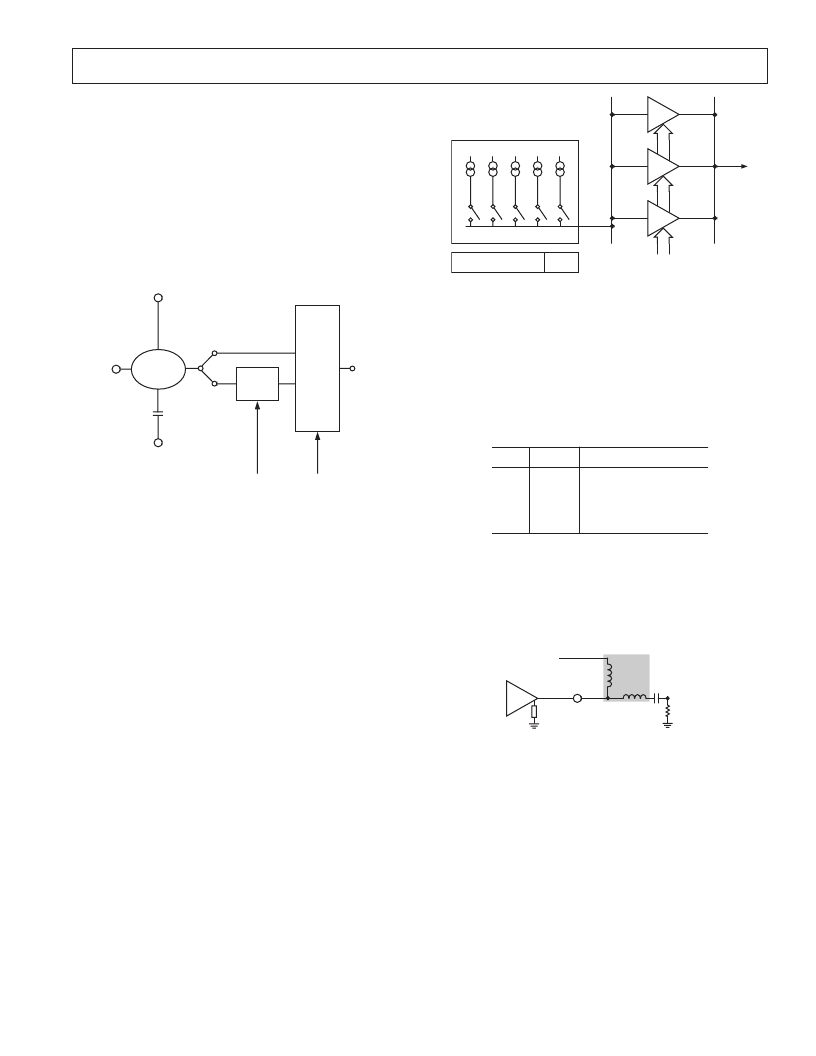
Voltage Controlled Oscillator (VCO)
An on-chip VCO is included on the transmitter. The VCO con-
verts the control voltage generated by the loop filter into an output
frequency that is sent to the antenna via the power amplifier
(PA). The VCO has a typical gain of 80 MHz/V and operates
from 866 MHz to 870 MHz. The PD1 bit in the function regis-
ter is the active high bit that turns on the VCO. A frequency
divided by 2 is included to allow operation in the lower 450 MHz
band. To enable operation in the lower band, the V1 bit in the
N Register should be set to 1.
The VCO needs an external 220 nF between the VCO and the
regulator to reduce internal noise.
MUX
VCO SELECT BIT
TO PA AND
N DIVIDER
DIVIDE
BY 2
VCO CONTROL BIT
LOOP FILTER
C
REG
PIN
220nF
VCO
Figure 7. Voltage Controlled Oscillator
RF Output Stage
The RF output stage consists of a DAC with a number of cur-
rent sources to adjust the output power level. To set up the
power level
FSK GFSK: The output power is set using the modulation
Register by entering a 7-bit number into Bits P1–P7. The
two MSBs set the range of the output stage, while the five
LSBs set the output power in the selected range.
ASK: The output power as set up for FSK is the output
power for a TxDATA of 1. The output power for a zero
data bit is set up the same way but using Bits D1–D7.
The output stage is powered down by setting Bit PD2 in the
function register to zero.
P5
P1
P7,
P6
HIGH
MED
LOW
Figure 8. Output Stage
Serial Interface
The serial interface allows the user to program the four 24-bit
registers using a 3-wire interface (CLK, Data, and Load Enable).
The serial interface consists of a level shifter, a 24-bit shift regis-
ter, and four latches. Signals should be CMOS compatible. The
serial interface is powered by the regulator, and therefore is
inactive when CE is low.
Table I. C2, C1 Truth Table
C2
C1
Data Latch
0
0
1
1
0
1
0
1
R Register
N Register
Modulation Register
Function Register
Data is clocked into the shift register, MSB first, on the rising
edge of each clock (CLK). Data is transferred to one of four
latches on the rising edge of LE. The destination latch is deter-
mined by the value of the two control bits (C2 and C1). These
are the two LSBs, DB1 and DB0, as shown in the timing dia-
gram of Figure 1.
V
DD
RF
OUT
PA
L1
C1
50
L2
Figure 9. Output Stage Matching
相關PDF資料 |
PDF描述 |
|---|---|
| ADF7011BRU | High Performance ISM Band ASK/FSK/GFSK Transmitter IC |
| ADF7011BRU-REEL | High Performance ISM Band ASK/FSK/GFSK Transmitter IC |
| ADF7011BRU-REEL7 | High Performance ISM Band ASK/FSK/GFSK Transmitter IC |
| ADF7020 | High Performance ISM Band FSK/ASK Transceiver IC |
| ADF7020BCP | High Performance ISM Band FSK/ASK Transceiver IC |
相關代理商/技術參數 |
參數描述 |
|---|---|
| ADF7011BRU | 制造商:Rochester Electronics LLC 功能描述: 制造商:Analog Devices 功能描述: |
| ADF7011BRU-REEL | 制造商:Rochester Electronics LLC 功能描述:ASK/FSK TRANSMITTER - Tape and Reel 制造商:Analog Devices 功能描述: |
| ADF7011BRU-REEL7 | 制造商:Rochester Electronics LLC 功能描述:ASK/FSK TRANSMITTER - Tape and Reel 制造商:Analog Devices 功能描述: |
| ADF7011BRUZ | 功能描述:IC XMITTER ASK/FSK/GFSK 24TSSOP RoHS:是 類別:RF/IF 和 RFID >> RF 發射器 系列:- 標準包裝:4,000 系列:- 頻率:310MHz ~ 440MHz 應用:- 調制或協議:UHF,ASK 數據傳輸率 - 最大:20 kBaud 功率 - 輸出:1dBm ~ 5dBm 電流 - 傳輸:10mA 數據接口:PCB,表面貼裝 天線連接器:PCB,表面貼裝 存儲容量:- 特點:- 電源電壓:2.2 V ~ 4 V 工作溫度:-40°C ~ 85°C 封裝/外殼:16-LSSOP(0.154",3.90mm 寬) 包裝:帶卷 (TR) |
| ADF7011BRUZ-RL | 功能描述:IC XMITTER ASK/FSK/GFSK 24TSSOP RoHS:是 類別:RF/IF 和 RFID >> RF 發射器 系列:- 標準包裝:4,000 系列:- 頻率:310MHz ~ 440MHz 應用:- 調制或協議:UHF,ASK 數據傳輸率 - 最大:20 kBaud 功率 - 輸出:1dBm ~ 5dBm 電流 - 傳輸:10mA 數據接口:PCB,表面貼裝 天線連接器:PCB,表面貼裝 存儲容量:- 特點:- 電源電壓:2.2 V ~ 4 V 工作溫度:-40°C ~ 85°C 封裝/外殼:16-LSSOP(0.154",3.90mm 寬) 包裝:帶卷 (TR) |
發布緊急采購,3分鐘左右您將得到回復。