- 您現(xiàn)在的位置:買賣IC網(wǎng) > PDF目錄373992 > ADG813 (Analog Devices, Inc.) REC3-SR_DR/H1 Series - Econoline Regulated DC-DC Converters; Input Voltage (Vdc): 05V; Output Voltage (Vdc): 15V; Power: 3W; Low Cost 3W converter in DIP24 Package; 1kVDC Isolation; Regulated Output; UL Approved; Continuous Short Circuit Protection; Internal SMD design; 3 Pinout Options, 3 Case Styles.; Efficiency to 75% PDF資料下載
參數(shù)資料
| 型號: | ADG813 |
| 廠商: | Analog Devices, Inc. |
| 元件分類: | DC/DC變換器 |
| 英文描述: | REC3-SR_DR/H1 Series - Econoline Regulated DC-DC Converters; Input Voltage (Vdc): 05V; Output Voltage (Vdc): 15V; Power: 3W; Low Cost 3W converter in DIP24 Package; 1kVDC Isolation; Regulated Output; UL Approved; Continuous Short Circuit Protection; Internal SMD design; 3 Pinout Options, 3 Case Styles.; Efficiency to 75% |
| 中文描述: | 0.5的CMOS 1.65 V至3.6 V四路SPST開關 |
| 文件頁數(shù): | 7/16頁 |
| 文件大小: | 392K |
| 代理商: | ADG813 |
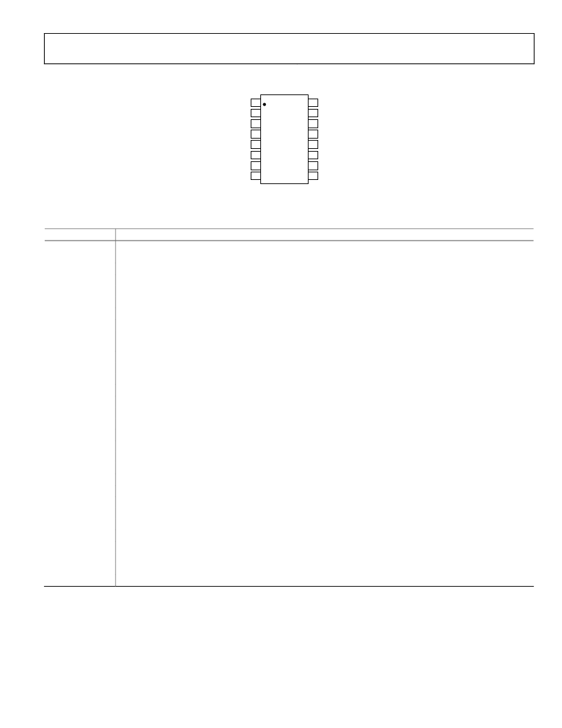
ADG811/ADG812/ADG813
PIN CONFIGURATION AND FUNCTION DESCRIPTIONS
Rev. A | Page 7 of 16
NC = NO CONNECT
NC
D1
S1
IN1
IN4
S4
D4
GND
D2
S2
VDD
IN2
S3
D3
IN3
NC
TOP VIEW
(Not to Scale)
ADG811/
ADG812/
ADG813
4
2
3
1
8
6
7
5
15
14
13
16
11
10
9
12
0
Figure 2.
Table 7. Terminology
Term
V
DD
I
DD
GND
S
D
IN
V
D
, V
S
R
ON
R
FLAT (ON)
Definition
Most positive power supply potential.
Positive supply current.
Ground (0 V) reference.
Source terminal. May be an input or output.
Drain terminal. May be an input or output.
Logic control input.
Analog voltage on Terminals D, S.
Ohmic resistance between D and S.
Flatness is defined as the difference between the maximum and minimum value of on resistance as measured over the
specified analog signal range.
On resistance match between any two channels, i.e., R
ON
max – R
ON
min.
Source leakage current with the switch off.
Drain leakage current with the switch off.
Channel leakage current with the switch on.
Maximum input voltage for Logic 0.
Minimum input voltage for Logic 1.
Input current of the digital input.
Off switch source capacitance. Measured with reference to ground.
Off switch drain capacitance. Measured with reference to ground.
On switch capacitance. Measured with reference to ground.
Digital input capacitance.
Delay time between the 50% and the 90% points of the digital input and switch on condition.
Delay time between the 50% and the 90% points of the digital input and switch off condition.
On or off time measured between the 80% points of both switches, when switching from one to another.
A measure of the glitch impulse transferred from the digital input to the analog output during on-to-off switching.
A measure of unwanted signal coupling through an off switch.
A measure of unwanted signal that is coupled through from one channel to another as a result of parasitic capacitance.
The frequency at which the output is attenuated by 3 dB.
The frequency response of the on switch.
The loss due to the on resistance of the switch.
The ratio of the harmonic amplitudes plus noise of a signal to the fundamental.
R
ON
I
S
(OFF)
I
D
(OFF)
I
D
, I
S
(ON)
V
INL
V
INH
I
INL
(I
INH
)
C
S
(OFF)
C
D
(OFF)
C
D
, C
S
(ON)
C
IN
t
ON
t
OFF
t
BBM
Charge Injection
Off Isolation
Crosstalk
–3 dB Bandwidth
On Response
Insertion Loss
THD + N
相關PDF資料 |
PDF描述 |
|---|---|
| ADG811YRU-REEL | 0.5 CMOS 1.65 V to 3.6 V Quad SPST Switches |
| ADG811YRU-REEL7 | 0.5 CMOS 1.65 V to 3.6 V Quad SPST Switches |
| ADG812YRU-REEL | 0.5 CMOS 1.65 V to 3.6 V Quad SPST Switches |
| ADG812YRU-REEL7 | 0.5 CMOS 1.65 V to 3.6 V Quad SPST Switches |
| ADG819BCB | 0.5 OHM CMOS 1.8 V to 5.5 V 2:1 Mux/SPDT Switches |
相關代理商/技術參數(shù) |
參數(shù)描述 |
|---|---|
| ADG813YRU | 功能描述:IC SWITCH QUAD SPST 16TSSOP RoHS:否 類別:集成電路 (IC) >> 接口 - 模擬開關,多路復用器,多路分解器 系列:- 標準包裝:1,000 系列:- 功能:多路復用器 電路:1 x 4:1 導通狀態(tài)電阻:- 電壓電源:雙電源 電壓 - 電源,單路/雙路(±):±5V 電流 - 電源:7mA 工作溫度:-40°C ~ 85°C 安裝類型:表面貼裝 封裝/外殼:16-SOIC(0.154",3.90mm 寬) 供應商設備封裝:16-SOIC 包裝:帶卷 (TR) |
| ADG813YRU-REEL | 功能描述:IC SWITCH QUAD SPST 16TSSOP RoHS:否 類別:集成電路 (IC) >> 接口 - 模擬開關,多路復用器,多路分解器 系列:- 標準包裝:1,000 系列:- 功能:多路復用器 電路:1 x 4:1 導通狀態(tài)電阻:- 電壓電源:雙電源 電壓 - 電源,單路/雙路(±):±5V 電流 - 電源:7mA 工作溫度:-40°C ~ 85°C 安裝類型:表面貼裝 封裝/外殼:16-SOIC(0.154",3.90mm 寬) 供應商設備封裝:16-SOIC 包裝:帶卷 (TR) |
| ADG813YRU-REEL7 | 功能描述:IC SWITCH QUAD SPST 16TSSOP RoHS:否 類別:集成電路 (IC) >> 接口 - 模擬開關,多路復用器,多路分解器 系列:- 標準包裝:1,000 系列:- 功能:多路復用器 電路:1 x 4:1 導通狀態(tài)電阻:- 電壓電源:雙電源 電壓 - 電源,單路/雙路(±):±5V 電流 - 電源:7mA 工作溫度:-40°C ~ 85°C 安裝類型:表面貼裝 封裝/外殼:16-SOIC(0.154",3.90mm 寬) 供應商設備封裝:16-SOIC 包裝:帶卷 (TR) |
| ADG813YRUZ | 功能描述:IC SWITCH QUAD SPST 16TSSOP RoHS:是 類別:集成電路 (IC) >> 接口 - 模擬開關,多路復用器,多路分解器 系列:- 應用說明:Ultrasound Imaging Systems Application Note 產(chǎn)品培訓模塊:Lead (SnPb) Finish for COTS Obsolescence Mitigation Program 標準包裝:250 系列:- 功能:開關 電路:單刀單擲 導通狀態(tài)電阻:48 歐姆 電壓電源:單電源 電壓 - 電源,單路/雙路(±):2.7 V ~ 5.5 V 電流 - 電源:5µA 工作溫度:0°C ~ 70°C 安裝類型:表面貼裝 封裝/外殼:48-LQFP 供應商設備封裝:48-LQFP(7x7) 包裝:托盤 |
| ADG819 | 制造商:AD 制造商全稱:Analog Devices 功能描述:0.5 OHM CMOS 1.8 V to 5.5 V 2:1 Mux/SPDT Switches |
發(fā)布緊急采購,3分鐘左右您將得到回復。