- 您現在的位置:買賣IC網 > PDF目錄373994 > ADL5519-EVALZ (Analog Devices, Inc.) 1 MHz to 10 GHz, 50 dB Dual Log Detector/Controller PDF資料下載
參數資料
| 型號: | ADL5519-EVALZ |
| 廠商: | Analog Devices, Inc. |
| 英文描述: | 1 MHz to 10 GHz, 50 dB Dual Log Detector/Controller |
| 中文描述: | 1兆赫至10 GHz,50分貝雙數檢波器/控制器 |
| 文件頁數: | 18/27頁 |
| 文件大小: | 479K |
| 代理商: | ADL5519-EVALZ |
第1頁第2頁第3頁第4頁第5頁第6頁第7頁第8頁第9頁第10頁第11頁第12頁第13頁第14頁第15頁第16頁第17頁當前第18頁第19頁第20頁第21頁第22頁第23頁第24頁第25頁第26頁第27頁
ADL5519
Preliminary Technical Data
and OUTP. This changes the output equation for OUTB and
OUTP to
Rev. PrB | Page 18 of 27
OUTB
= 2 ×
OUTA
VLVL
(14)
For VLVL < OUTA/2,
OUTN
= 0 V
(15)
Otherwise,
OUTN
= 2 ×
VLVL
–
OUTA
(16)
The previous equations are valid when Channel A is driven and
Channel B is slaved through a feedback loop. When Channel B
is driven and Channel A is slaved, the above equations can be
altered by changing OUTB to OUTA and OUTN to OUTP.
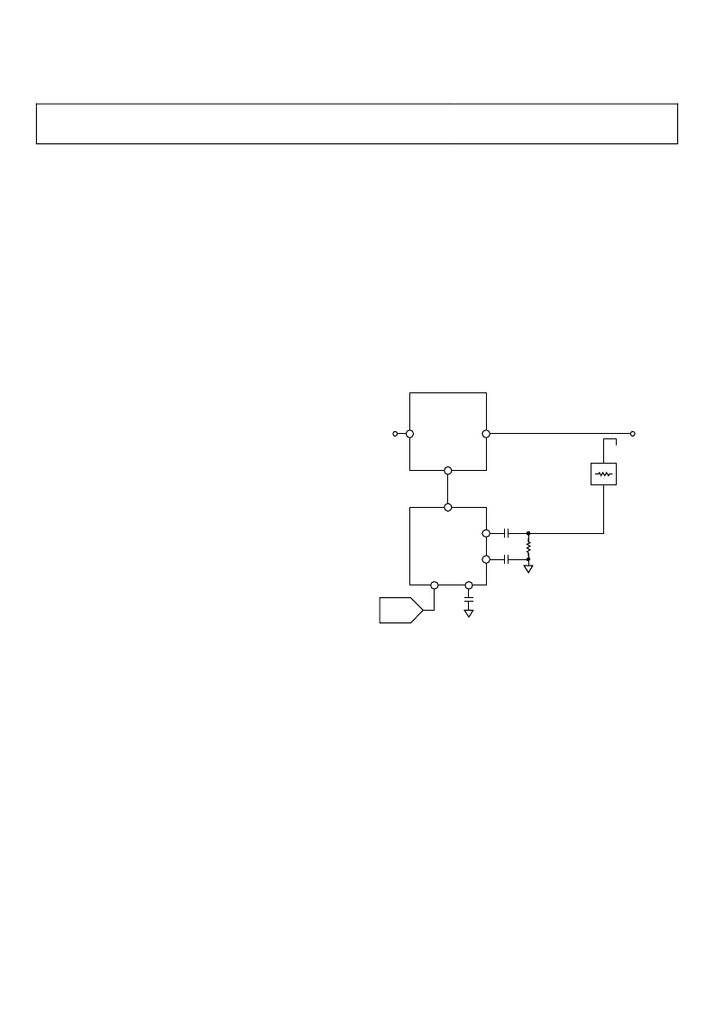
Automatic Power Control
Figure 20 shows how the device should be reconfigured to
control output
power
.
The RF input to the device is configured as before. A directional
coupler taps off some of the power being generated by the VGA
(typically a 10 dB to 20 dB coupler is used). A power splitter can
be used instead of a directional coupler if there are no concerns
about reflected energy from the next stage in the signal chain.
Some additional attenuation may be required to set the
maximum input signal at the ADL5519 to be equal to the
recommended maximum input level for optimum linearity and
temperature stability at the frequency of operation.
VSTA and OUTA are no longer shorted together. OUTA now
provides a bias or gain control voltage to the VGA. The gain
control sense of the VGA must be positive and monotonic, that
is, increasing voltage tends to increase gain. However, the gain
control transfer function of the device does not need to be well
controlled or particularly linear. If the gain control sense of the
VGA is negative, an inverting op amp circuit with a dc offset
shift can be used between the ADL5519 and the VGA to keep
the gain control voltage in the 0 V to 5 V range.
VSTA becomes the setpoint input to the system. This can be
driven by a DAC, as shown in Figure 20, if the output power is
expected to vary, or it can simply be driven by a stable reference
voltage if constant output power is required. This DAC should
have an output swing that covers the 0 V to 3.5 V range. The
AD7391 and AD7393 serial-input and parallel-input 10-bit
DACs provide adequate resolution (4 mV/bit) and an output
swing up to 4.5 V.
When VSTA is set to a particular value, the ADL5519 compares
this value to the equivalent input power present at the RF input.
If these two values do not match, OUTA increases or decreases
in an effort to balance the system. The dominant pole of the
error amplifier/integrator circuit that drives OUTA is set by the
capacitance on Pin CLPA; some experimentation may be
necessary to choose the right value for this capacitor. In general,
CLPA should be chosen to provide stable loop operation for the
complete output power control range. If the slope (in dB/V) of
the gain control transfer function of the VGA is not constant,
CLPA must be chosen to guarantee a stable loop when the gain
control slope is at its maximum. On the other hand, CLPA must
provide adequate averaging to the internal low range squaring
detector so that the rms computation is valid. Larger values of
CLPA tend to make the loop less responsive.
The relationship between VSTA and the RF input follows from
the measurement mode behavior of the device. For example,
from Figure 8, which shows the measurement mode transfer
function at 880 MHz, it can be seen that an input power of
10 dBm yields an output voltage of 2.5 V. Therefore, in
controller mode, VSTA should be set to 2.5 V, which results in
an input power of 10 dBm to the ADL5519.
ADL5519
VGA OR VVA
(OUTPUT POWER
INCREASES AS
V
APC
DECREASES)
V
APC
INHA
CLPA
INLA
0.1
μ
F
0.1
μ
F
SEE TEXT
VSTA
OUTA
DAC
0V TO 3.5V
(0V TO 4.9V AVAILABLE SWING)
P
IN
P
OUT
ATTENUATOR
50
Ω
Figure 20. Operation in Controller Mode for Automatic Power Control
Automatic Gain Control
Figure 21 shows how the ADL5519 can be connected to provide
automatic
gain
control to an amplifier or signal chain.
Additional pins are omitted for clarity. In this configuration,
both log detectors are connected in measurement mode with
appropriate filtering being used on CLP[A, B]. OUTA, however,
is also connected to the VLVL pin of the on-board difference
amplifier. Also, the OUTP output of the difference amplifier
drives a variable gain element (either VVA or VGA) and is
connected back to the FBKA input via a capacitor so that it is
operating as an integrator.
Assume that OUTA is much bigger than OUTB. Because OUTA
also drives VLVL, this voltage is also present on the noninverting
input of the op amp driving OUTP. This results in a net current
flow from OUTP through the integrating capacitor into the
FBKA input. This results in the voltage on OUTP decreasing. If
the gain control transfer function of the VVA/VGA is negative,
this increases the gain, which in turn increases the input signal
to INHB. The output voltage on the integrator continues to
相關PDF資料 |
PDF描述 |
|---|---|
| ADL5521-EVALZ | 400 MHz - 4 GHz Low Noise Amplifier |
| ADL5521 | 400 MHz - 4 GHz Low Noise Amplifier |
| ADL5521ACPZ-R7 | 400 MHz - 4 GHz Low Noise Amplifier |
| ADL5521ACPZ-WP | 400 MHz - 4 GHz Low Noise Amplifier |
| ADL5523-EVALZ | 400 MHz - 4 GHz Low Noise Amplifier |
相關代理商/技術參數 |
參數描述 |
|---|---|
| ADL5519XCPZ | 制造商:Analog Devices 功能描述:PREPRODUCTION DEVICES ADL5519 - Trays |
| ADL5521 | 制造商:AD 制造商全稱:Analog Devices 功能描述:400 MHz - 4000 MHz Low Noise Amplifier |
| ADL5521_08 | 制造商:AD 制造商全稱:Analog Devices 功能描述:400 MHz - 4000 MHz Low Noise Amplifier |
| ADL5521ACPZ | 制造商:Analog Devices 功能描述:SINGLE LNA WITH LOW GAIN - Rail/Tube |
| ADL5521ACPZ-R7 | 功能描述:IC AMP LNA 4GHZ LOW NOISE 8LFCSP RoHS:是 類別:RF/IF 和 RFID >> RF 放大器 系列:- 標準包裝:3,000 系列:- 頻率:100MHz ~ 6GHz P1dB:9.14dBm(8.2mW) 增益:15.7dB 噪音數據:1.3dB RF 型:CDMA,TDMA,PCS 電源電壓:2.7 V ~ 5 V 電流 - 電源:60mA 測試頻率:2GHz 封裝/外殼:0505(1412 公制) 包裝:帶卷 (TR) |
發布緊急采購,3分鐘左右您將得到回復。