- 您現在的位置:買賣IC網 > PDF目錄373995 > ADM1026JST-REEL (ANALOG DEVICES INC) Complete Thermal and System Management Controller PDF資料下載
參數資料
| 型號: | ADM1026JST-REEL |
| 廠商: | ANALOG DEVICES INC |
| 元件分類: | 電源管理 |
| 英文描述: | Complete Thermal and System Management Controller |
| 中文描述: | 4-CHANNEL POWER SUPPLY SUPPORT CKT, PQFP48 |
| 封裝: | 7 X 7 MM, 1.40 MM HEIGHT, PLASTIC, MS-026BBC, LQFP-48 |
| 文件頁數: | 19/56頁 |
| 文件大小: | 634K |
| 代理商: | ADM1026JST-REEL |
第1頁第2頁第3頁第4頁第5頁第6頁第7頁第8頁第9頁第10頁第11頁第12頁第13頁第14頁第15頁第16頁第17頁第18頁當前第19頁第20頁第21頁第22頁第23頁第24頁第25頁第26頁第27頁第28頁第29頁第30頁第31頁第32頁第33頁第34頁第35頁第36頁第37頁第38頁第39頁第40頁第41頁第42頁第43頁第44頁第45頁第46頁第47頁第48頁第49頁第50頁第51頁第52頁第53頁第54頁第55頁第56頁
ADM1026
Symmetrical bipolar input ranges can be accommodated easily
by making V
OS
equal to the full-scale voltage of the analog input,
and by adding a third resistor to set the positive full scale.
Rev. A | Page 19 of 56
R1
R2
V
IN
A
IN(0–9)
R3
+V
OS
0
Figure 30. Scaling and Offsetting A
IN0
A
IN9
for Bipolar Inputs
OS
fs
V
V
R2
R1
=
Note that R3 has no effect as the input voltage at the device pin
is zero when V
IN
= negative full scale.
(
IN0
A
R3
0
(
IN6
A
R3
5
)
(
)
IN5
fs
A
V
R1
to
for
0
=
)
(
)
IN9
fs
A
V
R1
to
for
5
=
Also, note that R2 has no effect as the input voltage at the device
pin is equal to V
OS
when V
IN
= positive full scale.
Battery Measurement Input (V
BAT
)
The V
BAT
input allows the condition of a CMOS backup battery
to be monitored. This is typically a lithium coin cell such as a
CR2032. The V
BAT
input is accurate only for voltages greater
than 1.5 V (see Figure 15). Typically, the battery in a system is
required to keep some device powered on when the system is in
a powered-off state. The V
BAT
measurement input is specially
designed to minimize battery drain. To reduce current drain
from the battery, the lower resistor of the V
BAT
attenuator is not
connected, except whenever a V
BAT
measurement is being made.
The total current drain on the V
BAT
pin is 80 nA typical (for a
maximum V
BAT
voltage = 4 V), so a CR2032 CMOS battery
functions in a system in excess of the expected 10 years. Note
that when a V
BAT
measurement is not being made, the current
drain is reduced to 6 nA typical. Under normal voltage meas-
urement operating conditions, all measurements are made in a
round-robin format, and each reading is actually the result of
16 digitally averaged measurements. However, averaging is not
carried out on the V
BAT
measurement to reduce measurement
time and therefore reduce the current drain from the battery.
The V
BAT
current drain when a measurement is being made is
calculated by
PERIOD
T
PULSE
T
BAT
k
V
I
×
=
Ω
100
For example, when
V
BAT
= 3 V,
A
n
78
ms
273
711
Ω
k
100
V
3
=
μ
×
=
s
I
where
T
PULSE
=
V
BAT
measurement time (711 μs typical),
T
PERIOD
= time to measure all analog inputs (273 ms typical),
and V
BAT
input battery protection.
V
BAT
Input Battery Protection
In addition to minimizing battery current drain, the V
BAT
measurement circuitry was specifically designed with battery
protection in mind. Internal circuitry prevents the battery from
being back-biased by the ADM1026 supply or through any
other path under normal operating conditions. In the unlikely
event of a catastrophic ADM1026 failure, the ADM1026
includes a second level of battery protection including a series
3 k resistor to limit current to the battery, as recommended by
UL. Thus, it is not necessary to add a series resistor between the
battery and the V
BAT
input; the battery can be connected directly
to the V
BAT
input to improve voltage measurement accuracy.
ADC
V
BAT
DIGITAL
CONTROL
49.5k
82.7k
4.5pF
3k
3k
0
Figure 31. Equivalent V
BAT
Input Protection Circuit
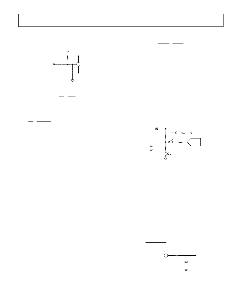
Reference Output (V
REF
)
The ADM1026 offers an on-chip reference voltage (Pin 24) that
can be used to provide a 1.82 V or 2.5 V reference voltage out-
put. This output is buffered and specified to sink or source a
load current of 2 mA. The reference voltage outputs 1.82 V if
Bit 2 of Configuration Register 3 (Address 07h) is 0; it outputs
2.5 V when this bit is set to 1. This voltage reference output can
be used to provide a stable reference voltage to external cir-
cuitry such as LDOs. The load regulation of the V
REF
output is
typically 0.15% for a sink current of 2 mA and 0.15% for 2 mA
source current. There may be some ripple present on the V
REF
output that requires filtering (±4 m V
MAX
). Figure 32 shows the
recommended circuitry for the V
REF
output for loads less than
2 mA. For loads in excess of 2 mA, external circuitry, such as
that shown in Figure 33, can be used to buffer the V
REF
output.
10k
0.1
μ
F
V
REF
ADM1026
24
V
REF
0
Figure 32. V
REF
Interface Circuit for V
REF
Loads < 2 mA
相關PDF資料 |
PDF描述 |
|---|---|
| ADM1026JSTZ-REEL | Complete Thermal and System Management Controller |
| ADM1026JST | Circular Connector; No. of Contacts:28; Series:LJT06R; Body Material:Aluminum; Connecting Termination:Crimp; Connector Shell Size:19; Circular Contact Gender:Pin; Circular Shell Style:Straight Plug; Insert Arrangement:19-28 |
| ADM1030ARQ | Intelligent Temperature Monitor and PWM Fan Controller |
| ADM1030 | Circular Connector; No. of Contacts:66; Series:LJT06R; Body Material:Aluminum; Connecting Termination:Crimp; Connector Shell Size:19; Circular Contact Gender:Socket; Circular Shell Style:Straight Plug; Insert Arrangement:19-35 |
| ADM1033 | Thermal Monitor and Fan Speed (RPM) Controller |
相關代理商/技術參數 |
參數描述 |
|---|---|
| ADM1026JST-REEL7 | 功能描述:IC CNTRL SYS REF/EEPROM 48LQFP RoHS:否 類別:集成電路 (IC) >> PMIC - 熱管理 系列:- 標準包裝:1 系列:- 功能:溫度監控系統(傳感器) 傳感器類型:內部和外部 感應溫度:-40°C ~ 125°C,外部傳感器 精確度:±2.5°C 本地(最大值),±5°C 遠程(最大值) 拓撲:ADC,比較器,寄存器庫 輸出類型:2 線 SMBus? 輸出警報:無 輸出風扇:無 電源電壓:2.7 V ~ 5.5 V 工作溫度:-40°C ~ 125°C 安裝類型:表面貼裝 封裝/外殼:SOT-23-8 供應商設備封裝:SOT-23-8 包裝:Digi-Reel® 其它名稱:296-22675-6 |
| ADM1026JSTZ | 功能描述:PMIC 解決方案 HI INT SYS MONITR IC RoHS:否 制造商:Texas Instruments 安裝風格:SMD/SMT 封裝 / 箱體:QFN-24 封裝:Reel |
| ADM1026JSTZ-R7 | 功能描述:PMIC 解決方案 HI INT SYS MONITR IC RoHS:否 制造商:Texas Instruments 安裝風格:SMD/SMT 封裝 / 箱體:QFN-24 封裝:Reel |
| ADM1026JSTZ-REEL | 功能描述:板上安裝溫度傳感器 HI INT SYS MONITR IC RoHS:否 制造商:Omron Electronics 輸出類型:Digital 配置: 準確性:+/- 1.5 C, +/- 3 C 溫度閾值: 數字輸出 - 總線接口:2-Wire, I2C, SMBus 電源電壓-最大:5.5 V 電源電壓-最小:4.5 V 最大工作溫度:+ 50 C 最小工作溫度:0 C 關閉: 安裝風格: 封裝 / 箱體: 設備功能:Temperature and Humidity Sensor |
| ADM1026JSTZ-REEL7 | 制造商:Analog Devices 功能描述:IC SYSTEM MONITOR 制造商:ON Semiconductor 功能描述:IC SYSTEM MONITOR |
發布緊急采購,3分鐘左右您將得到回復。