- 您現在的位置:買賣IC網 > PDF目錄373996 > ADM1066ASU (ANALOG DEVICES INC) Multisupply Supervisor/Sequencer with Margining Control and Auxiliary ADC Inputs PDF資料下載
參數資料
| 型號: | ADM1066ASU |
| 廠商: | ANALOG DEVICES INC |
| 元件分類: | 電源管理 |
| 英文描述: | Multisupply Supervisor/Sequencer with Margining Control and Auxiliary ADC Inputs |
| 中文描述: | 10-CHANNEL POWER SUPPLY SUPPORT CKT, PQFP48 |
| 封裝: | 7 X 7 MM, PLASTIC, MS-026ABC, TQFP-48 |
| 文件頁數: | 20/32頁 |
| 文件大小: | 861K |
| 代理商: | ADM1066ASU |
第1頁第2頁第3頁第4頁第5頁第6頁第7頁第8頁第9頁第10頁第11頁第12頁第13頁第14頁第15頁第16頁第17頁第18頁第19頁當前第20頁第21頁第22頁第23頁第24頁第25頁第26頁第27頁第28頁第29頁第30頁第31頁第32頁
ADM1066
VOLTAGE READBACK
The ADM1066 has an on-board 12-bit accurate ADC for
voltage readback over the SMBus. The ADC has a 12-channel
analog mux on the front end. The twelve channels consist of the
ten SFD inputs (VH, VP1-4, VX1-5) and two auxiliary (single-
ended) ADC inputs (AXU1, AUX2). Any or all of these inputs
can be selected to be read, in turn, by the ADC. The circuit
controlling this operation is called round-robin. The round-
robin circuit can be selected to run through its loop of conver-
sions just once or continuously. Averaging is also provided for
each channel. In this case, the round-robin circuit runs through
its loop of conversions 16 times before returning a result for
each channel. At the end of this cycle, the results are all written
to the output registers.
Rev. 0 | Page 20 of 32
The ADC samples single-sided inputs with respect to the AGND
pin. A 0 V input gives out Code 0, and an input equal to the
voltage on REFIN gives out full code (4095 decimal).
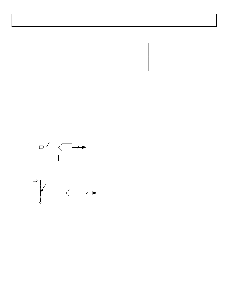
The inputs to the ADC come directly from the VXn pins and
from the back of the input attenuators on the VPn and VH pins,
as shown in Figure 30 and Figure 31.
0
VXn
2.048V VREF
NO ATTENUATION
12-BIT
ADC
DIGITIZED
VOLTAGE
READING
Figure 30. ADC Reading on VXn Pins
0
2.048V VREF
ATTENUATION NETWORK
(DEPENDS ON RANGE SELECTED)
12-BIT
ADC
DIGITIZED
VOLTAGE
READING
VPn/VH
Figure 31. ADC Reading on VPn/VH Pins
The voltage at the input pin can be derived from the following
equation:
V
=
4095
Code
ADC
×
Attenuation Factor
× 2.048 V
The ADC input voltage ranges for the SFD input ranges are
listed in Table 8.
Table 8. ADC Input Voltage Ranges
SFD Input
Range (V)
0.573–1.375
1.25–3
2.5–6
4.8–14.4
Attenuation Factor
1
2.181
4.363
10.472
ADC Input Voltage
Range (V)
0–2.048
0–4.46
0–6.0
1
0–14.4
1
_______________________________________________
1
The upper limit is the absolute maximum allowed voltage on these pins.
The normal way to supply the reference to the ADC on the
REFIN pin is to simply connect the REFOUT pin to the REFIN
pin. REFOUT provides a 2.048 V reference. As such, the
supervising range covers less than half of the normal ADC
range. It is possible, however, to provide the ADC with a more
accurate external reference for improved readback accuracy.
Supplies can also be connected to the input pins purely for ADC
readback, even though they might go above the expected super-
visory range limits (but not above 6 V, because this violates the
absolute maximum ratings on these pins). For instance, a 1.5 V
supply connected to the VX1 pin can be correctly read out as an
ADC code of approximately 3/4 full scale, but it always sits
above any supervisory limits that can be set on that pin. The
maximum setting for the REFIN pin is 2.048 V.
SUPPLY SUPERVISION WITH THE ADC
In addition to the readback capability, a further level of supervi-
sion is provided by the on-chip 12-bit ADC. The ADM1066 has
limit registers on which the user can program to a maximum or
minimum allowable threshold. Exceeding the threshold generates
a warning that can either be read back from the status registers
or input into the SE to determine what sequencing action the
ADM1066 should take. Only one register is provided for each
input channel, so a UV or OV threshold (but not both) can be
set for a given channel. The round-robin circuit can be enabled
via an SMBus write, or it can be programmed to turn on in any
state in the SE program. For example, it can be set to start once
a power-up sequence is complete and all supplies are known to
be within expected tolerance limits.
Note that a latency is built into this supervision, dictated by the
conversion time of the ADC. With all 12 channels selected, the
total time for the round-robin operation (averaging off) is
approximately 6 ms (500 μs per channel selected). Supervision
using the ADC, therefore, does not provide the same real time
response as the SFDs.
相關PDF資料 |
PDF描述 |
|---|---|
| ADM1069 | SUPER SEQUENCER-TM WITH MARGINING CONTROL AND AUXILIARY ADC INPUTS |
| ADM1069ACP | SUPER SEQUENCER-TM WITH MARGINING CONTROL AND AUXILIARY ADC INPUTS |
| ADM1069ACP-REEL | SUPER SEQUENCER-TM WITH MARGINING CONTROL AND AUXILIARY ADC INPUTS |
| ADM1069ACP-REEL7 | SUPER SEQUENCER-TM WITH MARGINING CONTROL AND AUXILIARY ADC INPUTS |
| ADM1070 | -48 V Hot Swap Controller |
相關代理商/技術參數 |
參數描述 |
|---|---|
| ADM1066ASU-REEL | 制造商:Analog Devices 功能描述:Volt Supervisor Sequencer 2.7V to 5.4V 48-Pin TQFP T/R |
| ADM1066ASU-REEL7 | 制造商:Analog Devices 功能描述:Volt Supervisor Sequencer 2.7V to 5.4V 48-Pin TQFP T/R |
| ADM1066ASU-U3 | 制造商:AD 制造商全稱:Analog Devices 功能描述:Multisupply Supervisor/Sequencer with Margining Control and Auxiliary ADC Inputs |
| ADM1066ASUZ | 功能描述:IC SUPERVISOR/SEQUENCER 48-TQFP RoHS:是 類別:集成電路 (IC) >> PMIC - 監控器 系列:Super Sequencer® 其它有關文件:STM6905 View All Specifications 標準包裝:1 系列:- 類型:多壓監控器 監視電壓數目:5 輸出:開路漏極或開路集電極 復位:低有效 復位超時:最小為 140 ms 電壓 - 閥值:2.188V,2.955V,可調,可調,可調 工作溫度:-40°C ~ 85°C 安裝類型:表面貼裝 封裝/外殼:8-TSSOP,8-MSOP(0.118",3.00mm 寬) 供應商設備封裝:8-TSSOP 包裝:Digi-Reel® 產品目錄頁面:1197 (CN2011-ZH PDF) 其它名稱:497-8728-6 |
| ADM1066ASUZ-REEL | 功能描述:IC SEQUENCER/SUPERVISOR 48TQFP RoHS:是 類別:集成電路 (IC) >> PMIC - 監控器 系列:Super Sequencer® 標準包裝:1 系列:- 類型:簡單復位/加電復位 監視電壓數目:1 輸出:開路漏極或開路集電極 復位:高有效 復位超時:- 電壓 - 閥值:1.8V 工作溫度:-40°C ~ 125°C 安裝類型:表面貼裝 封裝/外殼:6-TSOP(0.059",1.50mm 寬)5 引線 供應商設備封裝:5-TSOP 包裝:剪切帶 (CT) 其它名稱:NCP301HSN18T1GOSCT |
發布緊急采購,3分鐘左右您將得到回復。