- 您現在的位置:買賣IC網 > PDF目錄374015 > ADM8691 (Analog Devices, Inc.) Linear 1-cell Li-Ion Battery Charger w/Integrated FET, One LED 20-HTSSOP -20 to 70 PDF資料下載
參數資料
| 型號: | ADM8691 |
| 廠商: | Analog Devices, Inc. |
| 英文描述: | Linear 1-cell Li-Ion Battery Charger w/Integrated FET, One LED 20-HTSSOP -20 to 70 |
| 中文描述: | 微處理器監控電路 |
| 文件頁數: | 11/16頁 |
| 文件大小: | 207K |
| 代理商: | ADM8691 |
ADM8690–ADM8695
REV. 0
–11–
T Y PICAL APPLICAT IONS
ADM8690, ADM8692 and ADM8694
Figure 22a shows the ADM8690/ADM8692/ADM8694 in a
typical power monitoring, battery backup application. V
OUT
powers the CMOS RAM. Under normal operating conditions
with V
CC
present, V
OUT
is internally connected to V
CC
. If a
power failure occurs, V
CC
will decay and V
OUT
will be switched
to V
BAT T
thereby maintaining power for the CMOS RAM. A
RESET
pulse is also generated when V
CC
falls below 4.65 V for
the ADM8690/ADM8694 or 4.4 V for the ADM8692.
RESET
will remain low for 50 ms (200 ms for ADM8694) after V
CC
re-
turns to 5 V.
T he watchdog timer input (WDI) monitors an I/O line from the
μ
P system. T his line must be toggled once every 1.6 seconds to
verify correct software execution. Failure to toggle the line indi-
cates that the
μ
P system is not correctly executing its program
and may be tied up in an endless loop. If this happens, a reset
pulse is generated to initialize the processor.
If the watchdog timer is not needed, the WDI input should be
left floating.
T he Power Fail Input, PFI, monitors the input power supply via
a resistive divider network. T he voltage on the PFI input is com-
pared with a precision 1.3 V internal reference. If the input volt-
age drops below 1.3 V, a power fail output (
PFO
) signal is
generated. T his warns of an impending power failure and may
be used to interrupt the processor so that the system may be
shut down in an orderly fashion. T he resistors in the sensing
network are ratioed to give the desired power fail threshold
voltage V
T
.
V
T
=
(1.3
R
1/
R
2)
+
1.3
V
R
1/
R
2 = (
V
T
/1.3) – 1
+
BATTERY
R
1
R
2
+5V
0.1μF
ADM8690
ADM8692
ADM8694
V
CC
PFI
V
BATT
V
OUT
WDI
PFO
RESET
GND
μP POWER
CMOS RAM
POWER
μP SYSTEM
μP
RESET
μP NMI
I/O LINE
Figure 22a. ADM8690/ADM8692/ADM8694 Typical Applica-
tion Circuit A
Figure 22b shows a similar application but in this case the PFI
input monitors the unregulated input to the 7805 voltage regu-
lator. T his gives an earlier warning of an impending power fail-
ure. It is useful with processors operating at low speeds or where
there are a significant number of housekeeping tasks to be com-
pleted before the power is lost.
+
BATTERY
R
1
R
2
INPUT
POWER
V > 8V
0.1μF
0.1μF
7805
+5V
μP POWER
CMOS RAM
POWER
μP SYSTEM
μP
RESET
μP NMI
I/O LINE
ADM8690
ADM8692
ADM8694
V
CC
PFI
V
BATT
V
OUT
WDI
PFO
RESET
GND
Figure 22b. ADM8690/ADM8692/ADM8694 Typical Applica-
tion Circuit B
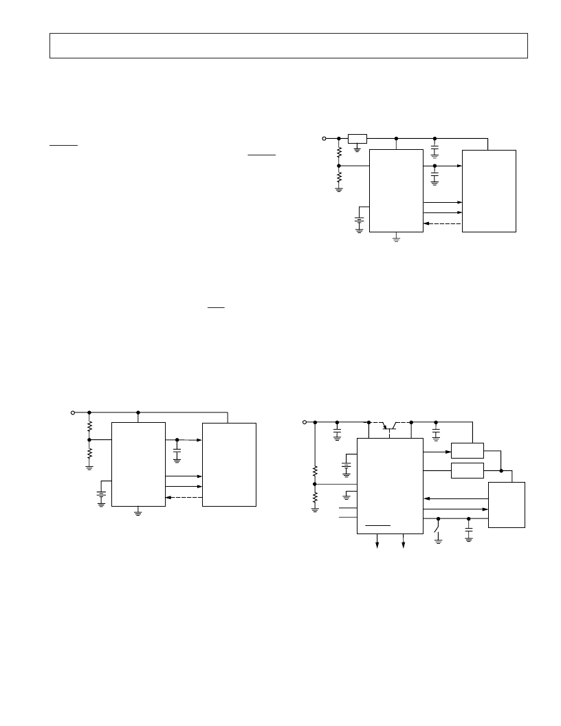
ADM8691, ADM8693 and ADM8695
A typical connection for the ADM8691/ADM8693/ADM8695
is shown in Figure 23. CMOS RAM is powered from V
OUT
.
When 5 V power is present this is routed to V
OUT
. If V
CC
fails
then V
BAT T
is routed to V
OUT
. V
OUT
can supply up to 100 mA
from V
CC
, but if more current is required, an external PNP tran-
sistor can be added. When V
CC
is higher than V
BAT T
, the BAT T
ON output goes low, providing up to 25 mA of base drive for
the external transistor. A 0.1
μ
F capacitor is connected to V
OUT
to supply the transient currents for CMOS RAM. When V
CC
is
lower than V
BAT T
, an internal 20
MOSFET connects the
backup battery to V
OUT
.
3V
BATTERY
R
1
R
2
0.1μF
0.1μF
0.1μF
RESET
SYSTEM STATUS
INDICATORS
NC
INPUT POWER
+5V
A0–A15
I/O LINE
NMI
RESET
μP
ADM8691
ADM8693
ADM8695
BATT
ON
V
CC
V
OUT
V
BATT
CE
OUT
CE
IN
PFI
GND
OSC IN
OSC SEL
WDI
PFO
RESET
LOW LINE
WDO
ADDRESS
DECODE
CMOS
RAM
Figure 23. ADM8691/ADM8693/ADM8695 Typical
Application
相關PDF資料 |
PDF描述 |
|---|---|
| ADM8691AN | Linear 1-cell Li-Ion Battery Charger w/Integrated FET, One LED 20-HTSSOP -20 to 70 |
| ADM8693 | bqTINY(TM) Linear 1-cell Li-Ion Charger w/ 1-A FET, AC Present and Temp Sense in QFN-10 10-SON -40 to 85 |
| ADM8693AN | bqTINY(TM) Linear 1-cell Li-Ion Charger w/ 1-A FET, AC Present & Charge Enable in QFN-10 10-SON -40 to 85 |
| ADM8695AN | bqTINY-II Dual Input USB/AC Adpater 1-Cell Li-Ion Charger w/Charge Enable & Temp Sense in QFN-10 10-SON -40 to 125 |
| ADM8695ARW | bqTINY-II Dual Input USB/AC Adpater 1-Cell Li-Ion Charger w/Charge Enable & Power Good in QFN-10 10-SON -40 to 125 |
相關代理商/技術參數 |
參數描述 |
|---|---|
| ADM8691AN | 制造商:Analog Devices 功能描述:Processor Supervisor 4.65V 4.75V to 5.5V 16-Pin PDIP 制造商:Rochester Electronics LLC 功能描述:IMPROVED ADM691 I.C. - Bulk 制造商:Analog Devices 功能描述:IC SUPERVISORY CCT 8691 DIP16 |
| ADM8691ANZ | 功能描述:IC SUPERVSR MPU 4.65V ADJ 16DIP RoHS:是 類別:集成電路 (IC) >> PMIC - 監控器 系列:- 標準包裝:1 系列:- 類型:簡單復位/加電復位 監視電壓數目:1 輸出:開路漏極或開路集電極 復位:高有效 復位超時:- 電壓 - 閥值:1.8V 工作溫度:-40°C ~ 125°C 安裝類型:表面貼裝 封裝/外殼:6-TSOP(0.059",1.50mm 寬)5 引線 供應商設備封裝:5-TSOP 包裝:剪切帶 (CT) 其它名稱:NCP301HSN18T1GOSCT |
| ADM8691ARN | 功能描述:IC SUPERVSR MPU 4.65V ADJ 16SOIC RoHS:否 類別:集成電路 (IC) >> PMIC - 監控器 系列:- 標準包裝:1 系列:- 類型:簡單復位/加電復位 監視電壓數目:1 輸出:開路漏極或開路集電極 復位:高有效 復位超時:- 電壓 - 閥值:1.8V 工作溫度:-40°C ~ 125°C 安裝類型:表面貼裝 封裝/外殼:6-TSOP(0.059",1.50mm 寬)5 引線 供應商設備封裝:5-TSOP 包裝:剪切帶 (CT) 其它名稱:NCP301HSN18T1GOSCT |
| ADM8691ARN-REEL | 功能描述:IC SUPERVSR MPU 4.65V ADJ 16SOIC RoHS:否 類別:集成電路 (IC) >> PMIC - 監控器 系列:- 標準包裝:1 系列:- 類型:簡單復位/加電復位 監視電壓數目:1 輸出:開路漏極或開路集電極 復位:高有效 復位超時:- 電壓 - 閥值:1.8V 工作溫度:-40°C ~ 125°C 安裝類型:表面貼裝 封裝/外殼:6-TSOP(0.059",1.50mm 寬)5 引線 供應商設備封裝:5-TSOP 包裝:剪切帶 (CT) 其它名稱:NCP301HSN18T1GOSCT |
| ADM8691ARNZ | 功能描述:IC SUPERVSR MPU 4.65V ADJ 16SOIC RoHS:是 類別:集成電路 (IC) >> PMIC - 監控器 系列:- 標準包裝:1 系列:- 類型:簡單復位/加電復位 監視電壓數目:1 輸出:開路漏極或開路集電極 復位:高有效 復位超時:- 電壓 - 閥值:1.8V 工作溫度:-40°C ~ 125°C 安裝類型:表面貼裝 封裝/外殼:6-TSOP(0.059",1.50mm 寬)5 引線 供應商設備封裝:5-TSOP 包裝:剪切帶 (CT) 其它名稱:NCP301HSN18T1GOSCT |
發布緊急采購,3分鐘左右您將得到回復。