- 您現在的位置:買賣IC網 > PDF目錄374015 > ADM8832ACP (ANALOG DEVICES INC) Charge Pump Regulator for Color TFT Panel PDF資料下載
參數資料
| 型號: | ADM8832ACP |
| 廠商: | ANALOG DEVICES INC |
| 元件分類: | 穩壓器 |
| 英文描述: | Charge Pump Regulator for Color TFT Panel |
| 中文描述: | SWITCHED CAPACITOR REGULATOR, 140 kHz SWITCHING FREQ-MAX, QCC20 |
| 封裝: | 4 X 4 MM, MO-220VGGD-1, LFCSP-20 |
| 文件頁數: | 6/12頁 |
| 文件大小: | 202K |
| 代理商: | ADM8832ACP |
ADM8832
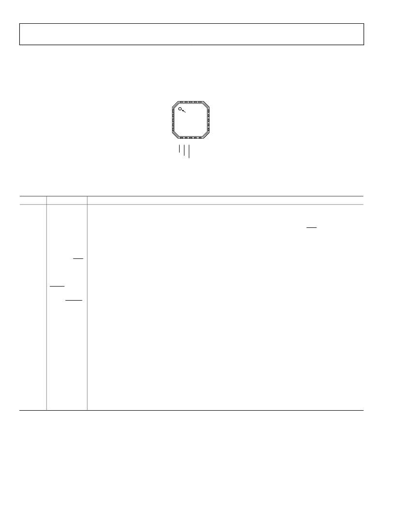
PIN CONFIGURATION AND FUNCTION DESCRIPTIONS
Rev. A | Page 6 of 12
0
15
C4–
C2+
C2–
C3+
C3–
11
14
13
12
1
2
3
4
5
2
6
7
8
9
1
+
C
S
S
L
+5VIN
+5VOUT
LDO_IN
VOUT
V
1
1
1
1
ADM8832
TOP VIEW
C
C
G
–
C
PIN 1
Figure 2. Pin Configuration
Table 4. Pin Function Descriptions
Pin No.
Mnemonic
1
V
CC
2
VOUT
Function
Positive Supply Voltage Input. Connect this pin to 3 V supply with a 2.2 μF decoupling capacitor.
Voltage Doubler Output. This is derived by doubling the 3 V supply. A 2.2 μF capacitor to ground is required on
this pin.
Voltage Regulator Input. The user has the option to bypass this circuit using the LDO_ON/OFF pin.
+5.1 V Output Pin. This is derived by doubling and regulating the +3 V supply. A 2.2 μF capacitor to ground is
required on this pin to stabilize the regulator.
+5.1 V Input Pin. This is the input to the voltage tripler and doubler inverter charge pump circuits.
Control Logic Input. 3 V CMOS logic. A logic high selects the internal LDO for regulation of the 5 V voltage
doubler output. A logic low isolates the internal LDO from the rest of the charge pump circuits. This allows the
use of an external LDO to regulate the 5 V voltage doubler output. The output of this LDO is then fed back into
the voltage tripler and doubler/inverter circuits of the ADM8832.
Digital Input. 3 V CMOS logic. Active low shutdown control. This pin shuts down the timing generator and
enables the discharge circuit to dissipate the charge on the voltage outputs, thus driving them to 0 V.
Drive Mode Input. 3 V CMOS logic. A logic high places the part in scan (high current) mode, and the charge
pump is driven by the internal oscillator. A logic low places the part in blanking (low current) mode, and the
charge pump is driven by the (slower) external oscillator. This is a power saving feature on the ADM8832.
External CLOCK Input. During a blanking period, the oscillator circuit selects this pin to drive the charge pump
circuit. This is at a lower frequency than the internal oscillator, resulting in lower quiescent current
consumption, thus saving power.
+15.3 V Output Pin. This is derived by tripling the +5.1 V regulated output. A 1 μF capacitor is required on
this pin.
External capacitor C3 is connected between these pins. A 1 μF capacitor is recommended.
External capacitor C2 is connected between these pins. A 1 μF capacitor is recommended.
External capacitor C4 is connected between these pins. A 1 μF capacitor is recommended.
10.2 V Output Pin. This is derived by doubling and inverting the +5.1 V regulated output. A 1 μF capacitor is
required on this pin.
Device Ground Pin.
External capacitor C1 is connected between these pins. A 2.2 μF capacitor is recommended.
3
4
LDO_IN
+5VOUT
5
6
+5VIN
LDO_ON/OFF
7
SHDN
8
SCAN/BLANK
9
CLKIN
10
+15VOUT
11, 12
13, 14
15, 16
17
C3, C3+
C2, C2+
C4, C4+
10VOUT
18
19, 20
GND
C1, C1+
相關PDF資料 |
PDF描述 |
|---|---|
| ADM8832ACP-REEL7 | Charge Pump Regulator for Color TFT Panel |
| ADM8832ACPZ1 | Charge Pump Regulator for Color TFT Panel |
| ADM8832ACP-REEL | Charge Pump Regulator for Color TFT Panel |
| ADM8832ACPZ-REEL | Charge Pump Regulator for Color TFT Panel |
| ADM8832ACPZ-REEL7 | Charge Pump Regulator for Color TFT Panel |
相關代理商/技術參數 |
參數描述 |
|---|---|
| ADM8832ACP-REEL | 制造商:AD 制造商全稱:Analog Devices 功能描述:Charge Pump Regulator for Color TFT Panel |
| ADM8832ACP-REEL7 | 制造商:AD 制造商全稱:Analog Devices 功能描述:Charge Pump Regulator for Color TFT Panel |
| ADM8832ACPZ | 功能描述:IC CHARGE PUMP REG TFT 20LFCSP RoHS:是 類別:集成電路 (IC) >> PMIC - 穩壓器 - 專用型 系列:- 標準包裝:43 系列:- 應用:控制器,Intel VR11 輸入電壓:5 V ~ 12 V 輸出數:1 輸出電壓:0.5 V ~ 1.6 V 工作溫度:-40°C ~ 85°C 安裝類型:表面貼裝 封裝/外殼:48-VFQFN 裸露焊盤 供應商設備封裝:48-QFN(7x7) 包裝:管件 |
| ADM8832ACPZ1 | 制造商:AD 制造商全稱:Analog Devices 功能描述:Charge Pump Regulator for Color TFT Panel |
| ADM8832ACPZ-REEL | 功能描述:IC CHARGE PUMP REG TFT 20LFCSP RoHS:是 類別:集成電路 (IC) >> PMIC - 穩壓器 - 專用型 系列:- 標準包裝:43 系列:- 應用:控制器,Intel VR11 輸入電壓:5 V ~ 12 V 輸出數:1 輸出電壓:0.5 V ~ 1.6 V 工作溫度:-40°C ~ 85°C 安裝類型:表面貼裝 封裝/外殼:48-VFQFN 裸露焊盤 供應商設備封裝:48-QFN(7x7) 包裝:管件 |
發布緊急采購,3分鐘左右您將得到回復。