- 您現在的位置:買賣IC網 > PDF目錄374016 > ADMC401BST (ANALOG DEVICES INC) Single-Chip, DSP-Based High Performance Motor Controller PDF資料下載
參數資料
| 型號: | ADMC401BST |
| 廠商: | ANALOG DEVICES INC |
| 元件分類: | 數字信號處理 |
| 英文描述: | Single-Chip, DSP-Based High Performance Motor Controller |
| 中文描述: | 24-BIT, 13 MHz, OTHER DSP, PQFP144 |
| 封裝: | PLASTIC, LQFP-144 |
| 文件頁數: | 24/60頁 |
| 文件大小: | 417K |
| 代理商: | ADMC401BST |
第1頁第2頁第3頁第4頁第5頁第6頁第7頁第8頁第9頁第10頁第11頁第12頁第13頁第14頁第15頁第16頁第17頁第18頁第19頁第20頁第21頁第22頁第23頁當前第24頁第25頁第26頁第27頁第28頁第29頁第30頁第31頁第32頁第33頁第34頁第35頁第36頁第37頁第38頁第39頁第40頁第41頁第42頁第43頁第44頁第45頁第46頁第47頁第48頁第49頁第50頁第51頁第52頁第53頁第54頁第55頁第56頁第57頁第58頁第59頁第60頁
REV. B
ADMC401
–24–
CONVERT START COMMAND
The analog-to-digital conversion process of the ADMC401 may
be started by either an internal or an external command. Bit 0 of
the ADCCTRL register determines whether internal or external
convert start mode is enabled. If Bit 0 of the ADCCTRL regis-
ter is cleared, internal convert start mode is selected, and the
ADC conversion process is started on the rising edge of the
PWMSYNC signal. This results in one conversion sequence per
PWM switching period (at the start of each period) when the
PWM generation unit operates in the single update mode. In the
double update operating mode, there are two conversion se-
quences per PWM switching period (one at the start and one in
the middle of each period). In internal convert start mode, in
order to ensure correct synchronization and jitter-free operation,
it is essential that the value written to the PWMTM register be a
multiple of four. In other words, the two LSBs of the value
written to the PWMTM register must both be 0.
If Bit 0 of the ADCCTRL register is set, external convert start
mode is selected. In this mode, the conversion process is started
on the occurrence of a rising edge on the CONVST pin. Addi-
tionally, the start of conversion can be placed under software
control by externally connecting one of the programmable input/
output (PIO) lines to the CONVST pin and generating a rising
edge by writing to the appropriate bit of the PIODATA register.
By default, following reset, Bit 0 of the ADCCTRL register is
cleared so that internal convert start mode is selected.
ADC CLOCK SIGNALS
The ADC consists of a pipeline flash architecture and is clocked
at a quarter of the DSP instruction rate. All of the timing of the
ADC system (including control of the multiplexers and sample
and hold amplifiers) is regulated by this clock signal and it de-
termines the total conversion time for all of the channels as well
as the delay between sampling of successive pairs of analog
inputs. The ADC clock rate is internally fixed and may not be
changed. The period of the ADC clock, t
CKADC
is related to the
DSP CLKOUT period by:
t
t
CKADC
CK
=
×
4
A DSP rate of 26 MHz corresponds to a
t
CKADC
of approxi-
mately 154 ns.
ANALOG INPUT CONFIGURATION AND OVERVIEW
Figure 17 is a simplified model of the ADC input structure for
one channel (VIN0) of the ADC system of the ADMC401. This
model applies to all eight input channels. The internal multi-
plexers are used to switch the various analog inputs to the A/D
converter. For analog inputs VIN0 to VIN3, there is a single
common terminal (ASHAN) that is the inverting input to the
internal differential sample and hold amplifier. For the input
signals, VIN4 to VIN7, the equivalent input is BSHAN. The
value V
REF
(internally generated voltage reference or externally
applied voltage reference on the V
REF
pin) defines the maximum
input voltage to the A/D core. The minimum input voltage to
the A/D core is automatically defined as –V
REF
.
+V
REF
–
V
REF
12
VIN0
ASHAN
V
CORE
A/D
CORE
Figure 17. Equivalent Functional Input Circuit of ADC
System
The dc voltage on the V
REF
pin sets the common-mode voltage
of the A/D converter of the ADMC401. For example, when
using the internal 2.0 V reference, the input level will also be
centered about 2.0 V. The ADC inputs of the ADMC401 can
be configured for single ended operation, where the inverting
terminals (ASHAN and BSHAN) are connected directly to the
reference voltage level, and the analog inputs (VIN0 to VIN7)
are driven by analog signals with a 4.0 V p-p range. The VIN0
to VIN7 inputs are unipolar so that when operating from the
internal 2.0 V reference, these signals can range from 0 V to
4 V. The recommended single-ended input configuration for a
single analog input channel of the ADMC401 is shown in Fig-
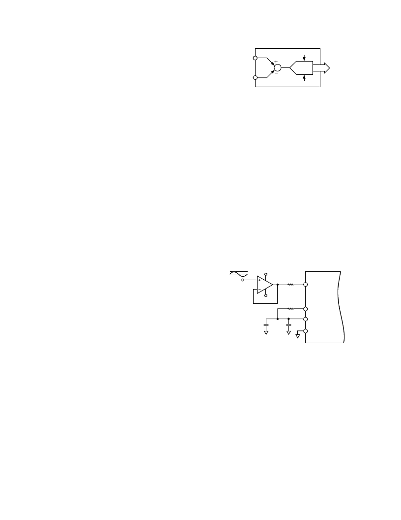
ure 18. The input to the A/D converter must be driven by an
operational amplifier with sufficient drive strength so that the
A/D performance is not degraded. Sufficient drive strength is
the ability to drive a load of 6 pF static and 4 pF switched from
ground (capacitive) to settle within
±
1.0 mV within 70 ns. In
Figure 18, the operational amplifier is shown configured as a
simple noninverting input buffer. Of course, the operational
amplifier stage could also be used to implement any necessary
level shifting and/or filtering of the input signal.
+V
–
V
VIN0
ASHAN
V
REF
SENSE
ADMC401
R
S
R
S
10 F
0.1 F
4V
0V
Figure 18. Typical Single-Ended Input Configuration for
ADMC401
From Figure 17, it is clear that the input to the A/D core is
simply given by:
V
VIN
ASHAN
CORE
=
0–
which must satisfy the condition:
–
V
V
V
REF
CORE
REF
≤
≤
where
V
REF
is the voltage at the V
REF
pin of the ADMC401
(either internally generated or externally supplied). There is an
additional limit placed on the valid operating range for the VIN0
and ASHAN inputs that is bounded by the power supply of the
ADMC401:
AV
AV
V
VIN
AV
V
V
ASHAN
AV
V
SS
DD
SS
DD
–0 3
.
–0 3
.
0
0 3
0 3
≤
≤
+
≤
≤
+
相關PDF資料 |
PDF描述 |
|---|---|
| ADMC401 | Single-Chip, DSP-Based High Performance Motor Controller |
| ADMC401-ADVEVALKIT | Circular Connector; No. of Contacts:5; Series:MS27497; Body Material:Aluminum; Connecting Termination:Crimp; Connector Shell Size:10; Circular Contact Gender:Pin; Circular Shell Style:Wall Mount Receptacle; Insert Arrangement:10-5 RoHS Compliant: No |
| ADMC401-PB | Single-Chip, DSP-Based High Performance Motor Controller |
| ADMCF340 | DashDSPTM 64-Lead Flash Mixed-Signal DSP with Enhanced Analog Front End |
| ADMCF340BST | DashDSPTM 64-Lead Flash Mixed-Signal DSP with Enhanced Analog Front End |
相關代理商/技術參數 |
參數描述 |
|---|---|
| ADMC401BSTZ | 功能描述:IC DSP 8CH 12BIT MOTCTRL 144LQFP RoHS:是 類別:集成電路 (IC) >> 嵌入式 - DSP(數字式信號處理器) 系列:電機控制 標準包裝:2 系列:StarCore 類型:SC140 內核 接口:DSI,以太網,RS-232 時鐘速率:400MHz 非易失內存:外部 芯片上RAM:1.436MB 電壓 - 輸入/輸出:3.30V 電壓 - 核心:1.20V 工作溫度:-40°C ~ 105°C 安裝類型:表面貼裝 封裝/外殼:431-BFBGA,FCBGA 供應商設備封裝:431-FCPBGA(20x20) 包裝:托盤 |
| ADMC401BSTZKL1 | 制造商:Analog Devices 功能描述: |
| ADMC401-PB | 制造商:AD 制造商全稱:Analog Devices 功能描述:Single-Chip, DSP-Based High Performance Motor Controller |
| ADMCF326 | 制造商:AD 制造商全稱:Analog Devices 功能描述:28-Lead Flash Memory DSP Motor Controller |
| ADMCF326BN | 制造商:Analog Devices 功能描述: |
發布緊急采購,3分鐘左右您將得到回復。