- 您現(xiàn)在的位置:買賣IC網(wǎng) > PDF目錄374016 > ADMC401BST (ANALOG DEVICES INC) Single-Chip, DSP-Based High Performance Motor Controller PDF資料下載
參數(shù)資料
| 型號: | ADMC401BST |
| 廠商: | ANALOG DEVICES INC |
| 元件分類: | 數(shù)字信號處理 |
| 英文描述: | Single-Chip, DSP-Based High Performance Motor Controller |
| 中文描述: | 24-BIT, 13 MHz, OTHER DSP, PQFP144 |
| 封裝: | PLASTIC, LQFP-144 |
| 文件頁數(shù): | 41/60頁 |
| 文件大小: | 417K |
| 代理商: | ADMC401BST |
第1頁第2頁第3頁第4頁第5頁第6頁第7頁第8頁第9頁第10頁第11頁第12頁第13頁第14頁第15頁第16頁第17頁第18頁第19頁第20頁第21頁第22頁第23頁第24頁第25頁第26頁第27頁第28頁第29頁第30頁第31頁第32頁第33頁第34頁第35頁第36頁第37頁第38頁第39頁第40頁當前第41頁第42頁第43頁第44頁第45頁第46頁第47頁第48頁第49頁第50頁第51頁第52頁第53頁第54頁第55頁第56頁第57頁第58頁第59頁第60頁
ADMC401
–41–
REV. B
ETU REGISTERS
The configuration of the ETU registers is shown at the end of
the data sheet.
AUXILIARY PWM TIMERS
The ADMC401 provides two variable-frequency, variable duty-
cycle, 8-bit, auxiliary PWM outputs that are available at the
AUX1 and AUX0 pins. These auxiliary PWM outputs can be
used to provide switching signals to other circuits in a typical
motor control system such as power factor corrected front-end
converters or other switching power converters. Alternatively,
by addition of a suitable filter network, the auxiliary PWM out-
put signals can be used as simple single-bit digital-to-analog
converters.
The auxiliary PWM system of the ADMC401 can operate in
two different modes,
independent mode
or
offset mode
. The oper-
ating mode of the auxiliary PWM system is controlled by Bit 8
of the MODECTRL register. Setting Bit 8 of the MODECTRL
register places the auxiliary PWM system in the independent
mode. In this mode, the two auxiliary PWM generators are
completely independent, and separate switching frequencies and
duty cycles may be programmed for each auxiliary PWM out-
put. In this mode, the 8-bit AUXTM0 register sets the switch-
ing frequency of the signal at the AUX0 output pin. Similarly,
the 8-bit AUXTM1 register sets the switching frequency of the
signal at the AUX1 pin. The fundamental time increment for
the auxiliary PWM outputs is twice the DSP instruction rate (or
2t
CK
) so that the corresponding switching periods are given by:
T
T
AUXTM
t
AUXTM
t
AUX
CK
AUX
CK
0
1
2
0
1
2
1
1
=
×
+
×
=
×
+
×
(
)
(
)
Since the values in both AUXTM0 and AUXTM1 can range
from 0 to 0xFF, the achievable switching frequency of the auxil-
iary PWM signals may range from 50.8 kHz to 13 MHz for a
CLKOUT frequency of 26 MHz.
The on-time of the two auxiliary PWM signals are programmed
by the two 8-bit AUXCH0 and AUXCH1 registers, according
to:
T
AUXCH
t
T
AUXCH
t
ON AUX
,
CK
ON AUX
,
CK
0
1
2
0
2
1
=
×
×
=
×
×
so that output duty cycles from 0% to 100% are possible. Duty
cycles of 100% are produced if the on-time value exceeds the
period value. Typical auxiliary PWM waveforms in independent
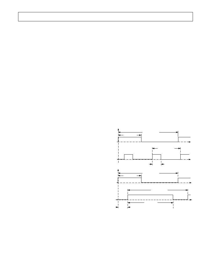
mode are shown in Figure 33(a).
When Bit 8 of the MODECTRL register is cleared, the auxiliary
PWM channels are placed in offset mode. In offset mode, the
switching frequency of the two signals on the AUX0 and AUX1
pins are identical and controlled by AUXTM0 in a manner
similar to that previously described for independent mode. The
on-times of both the AUX0 and AUX1 signals are controlled by
the AUXCH0 and AUXCH1 registers as before. However, in
this mode, the AUXTM1 register defines the offset time from
the rising edge of the signal on the AUX0 pin to that on the
AUX1 pin, according to:
T
AUXTM
t
OFFSET
CK
= ×
2
×
1 1
(
)
For correct operation in this mode, the value written to the
AUXTM1 register
must be
less than the value written to the
AUXTM0 register. Typical auxiliary PWM waveforms in offset
mode are shown in Figure (33)b. Again, duty cycles from 0% to
100% are possible in this mode.
In both operating modes, the resolution of the auxiliary PWM
system is 8-bit
only
at the minimum switching frequency
(AUXTM0 = AUXTM1 = 255 in independent mode, AUXTM0
= 255 in offset mode). Obviously, as the switching frequency is
increased, the resolution is reduced.
Values can be written to the auxiliary PWM registers at any
time. However, new duty cycle values written to the AUXCH0
and AUXCH1 registers only become effective at the start of the
next cycle. Writing to the AUXTM0 and AUXTM1 registers
causes the internal timers to be reset to 0 and new PWM cycles
to begin, only in independent mode.
By default, following reset, Bit 8 of the MODECTRL
register is cleared and offset mode is enabled. AUXTM0 and
AUXTM1 default to 0xFF corresponding to minimum switch-
ing frequency and zero offset. The on-time registers AUXCH0
and AUXCH1 default to 0x00.
2
AUXCH0
2
AUXCH0
(a)
(b)
AUX0
AUX1
AUX0
AUX1
2
(AUXTM0+1)
2
(AUXTM1+1)
2
AUXCH1
2
(AUXTM0+1)
2
(AUXTM1+1)
2
(AUXTM0+1)
2
AUXCH1
Figure 33. Typical Auxiliary PWM Signals in (a) Indepen-
dent Mode and (b) Offset Mode
AUXILIARY PWM REGISTERS
The registers of the auxiliary PWM system are illustrated at the
end of the data sheet.
相關(guān)PDF資料 |
PDF描述 |
|---|---|
| ADMC401 | Single-Chip, DSP-Based High Performance Motor Controller |
| ADMC401-ADVEVALKIT | Circular Connector; No. of Contacts:5; Series:MS27497; Body Material:Aluminum; Connecting Termination:Crimp; Connector Shell Size:10; Circular Contact Gender:Pin; Circular Shell Style:Wall Mount Receptacle; Insert Arrangement:10-5 RoHS Compliant: No |
| ADMC401-PB | Single-Chip, DSP-Based High Performance Motor Controller |
| ADMCF340 | DashDSPTM 64-Lead Flash Mixed-Signal DSP with Enhanced Analog Front End |
| ADMCF340BST | DashDSPTM 64-Lead Flash Mixed-Signal DSP with Enhanced Analog Front End |
相關(guān)代理商/技術(shù)參數(shù) |
參數(shù)描述 |
|---|---|
| ADMC401BSTZ | 功能描述:IC DSP 8CH 12BIT MOTCTRL 144LQFP RoHS:是 類別:集成電路 (IC) >> 嵌入式 - DSP(數(shù)字式信號處理器) 系列:電機控制 標準包裝:2 系列:StarCore 類型:SC140 內(nèi)核 接口:DSI,以太網(wǎng),RS-232 時鐘速率:400MHz 非易失內(nèi)存:外部 芯片上RAM:1.436MB 電壓 - 輸入/輸出:3.30V 電壓 - 核心:1.20V 工作溫度:-40°C ~ 105°C 安裝類型:表面貼裝 封裝/外殼:431-BFBGA,F(xiàn)CBGA 供應(yīng)商設(shè)備封裝:431-FCPBGA(20x20) 包裝:托盤 |
| ADMC401BSTZKL1 | 制造商:Analog Devices 功能描述: |
| ADMC401-PB | 制造商:AD 制造商全稱:Analog Devices 功能描述:Single-Chip, DSP-Based High Performance Motor Controller |
| ADMCF326 | 制造商:AD 制造商全稱:Analog Devices 功能描述:28-Lead Flash Memory DSP Motor Controller |
| ADMCF326BN | 制造商:Analog Devices 功能描述: |
發(fā)布緊急采購,3分鐘左右您將得到回復(fù)。