- 您現在的位置:買賣IC網 > PDF目錄374016 > ADMCF340-EVALKIT (Analog Devices, Inc.) Circular Connector; No. of Contacts:7; Series:MS27497; Body Material:Aluminum; Connecting Termination:Crimp; Connector Shell Size:10; Circular Contact Gender:Pin; Circular Shell Style:Wall Mount Receptacle; Insert Arrangement:10-99 RoHS Compliant: No PDF資料下載
參數資料
| 型號: | ADMCF340-EVALKIT |
| 廠商: | Analog Devices, Inc. |
| 元件分類: | 圓形連接器 |
| 英文描述: | Circular Connector; No. of Contacts:7; Series:MS27497; Body Material:Aluminum; Connecting Termination:Crimp; Connector Shell Size:10; Circular Contact Gender:Pin; Circular Shell Style:Wall Mount Receptacle; Insert Arrangement:10-99 RoHS Compliant: No |
| 中文描述: | DashDSPTM 64無鉛閃存混合信號增強的DSP與模擬前端 |
| 文件頁數: | 12/40頁 |
| 文件大小: | 415K |
| 代理商: | ADMCF340-EVALKIT |
第1頁第2頁第3頁第4頁第5頁第6頁第7頁第8頁第9頁第10頁第11頁當前第12頁第13頁第14頁第15頁第16頁第17頁第18頁第19頁第20頁第21頁第22頁第23頁第24頁第25頁第26頁第27頁第28頁第29頁第30頁第31頁第32頁第33頁第34頁第35頁第36頁第37頁第38頁第39頁第40頁
REV. 0
ADMCF340
–12–
Reset
The ADMCF340 DSP core and peripherals must be correctly
reset when the device is powered up to assure proper unitization.
The ADMCF340 contains an integrated power-on-reset (POR)
circuit that provides a complete system reset on power-up and
power-down. The POR circuit monitors the voltage on the
ADMCF340 V
DD
Pin and holds the DSP core and peripherals
in reset while V
DD
is less than the threshold voltage level, V
RST
.
When this voltage is exceeded, the ADMCF340 is held in reset
for an additional 2
16
DSP clock cycles (T
RST
in Figure 5). During
this time (T
RST
), the supply voltage must reach the recommended
operating condition. On power-down, when the voltage on the
V
DD
Pin falls below V
RST
–V
HYST
, the ADMCF340 will be
reset. Also, if the external
RESET
Pin is actively pulled low
at any time after power-up, a complete hardware reset of the
ADMCF340 is initiated.
V
RST
V
DD
RESET
V
RST –
V
HYST
T
RST
Figure 5. Power-On Reset Operation
The ADMCF340 sets all internal stack pointers to the empty
stack condition, masks all interrupts, clears the MSTAT Register,
and performs a full reset of all the motor control peripherals.
Following a power-up, it is possible to initiate a DSP core and
motor control peripheral reset by pulling the
RESET
Pin low.
The
RESET
signal must be the minimum pulsewidth specification,
t
RSP
. Following the reset sequence, the DSP core starts executing
code from the internal PM ROM located at 0x0800.
DSP Control Registers
The DSP core has a system control register, SYSCNTL, memory-
mapped at DM (0x3FFF). SPORT1 must be configured as a
serial port by setting Bit 10. SPORT0 and SPORT1 are enabled
by setting Bit 11 and Bit 12.
The DSP core has a wait state control register, MEMWAIT,
memory-mapped at DM (0x3FFE). The default value of this
register is 0xFFFF. For proper operation of the ADMCF340,
this register must always contain the value 0x8000. This value
sets the minimum access time to the program memory.
The configurations of both the SYSCNTL and MEMWAIT Reg-
isters of the ADMCF340 are shown at the end of the data sheet.
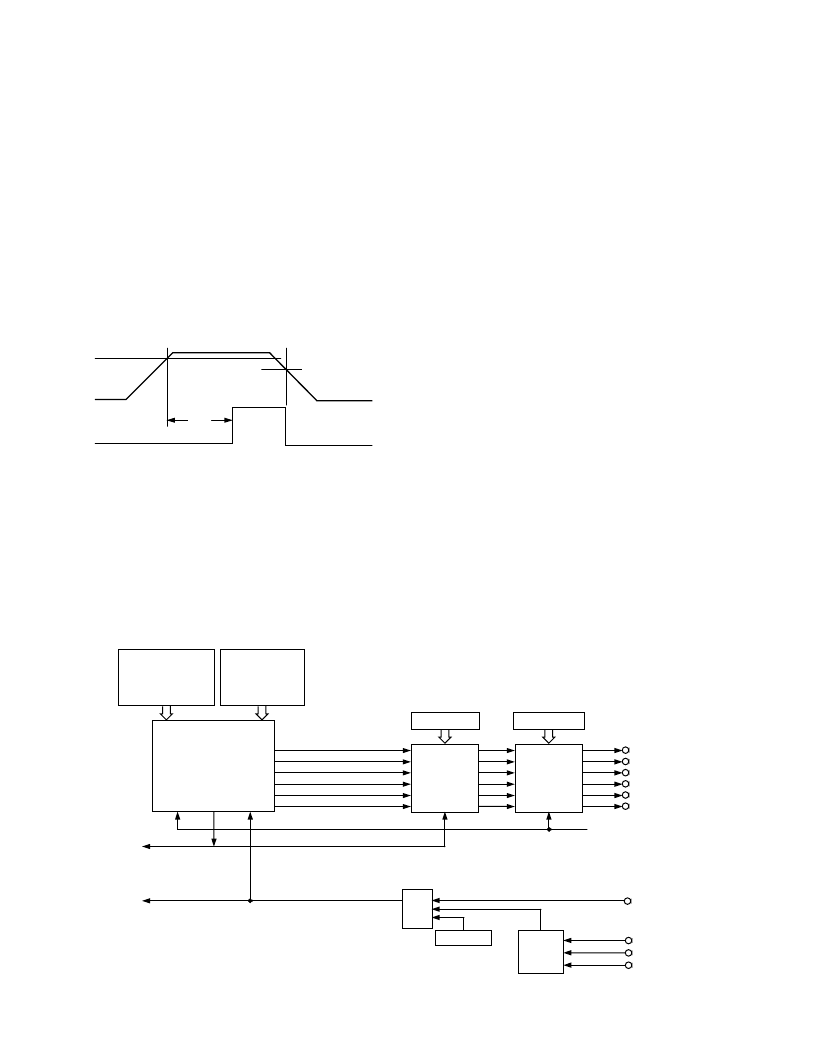
THREE-PHASE PWM CONTROLLER
Overview
The PWM generator block of the ADMCF340 is a flexible,
programmable, three-phase PWM waveform generator that can
be programmed to generate the required switching patterns to
drive a three-phase voltage source inverter for ac induction motors
(ACIM) or permanent magnet synchronous motors (PMSM).
In addition, the PWM block contains special functions that
considerably simplify the generation of the required PWM
switching patterns for control of electronically commutated
motors (ECM), brushless dc motors (BDCM), or switched
reluctance motors (SRM).
The six PWM output signals consist of three high side drive
signals (AH, BH, and CH) and three low side drive signals (AL,
BL, and CL). The switching frequency, dead time, and minimum
pulsewidths of the generated PWM patterns are programmable
using, respectively, the PWMTM, PWMDT, and PWMPD
registers. In addition, three registers (PWMCHA, PWMCHB,
and PWMCHC) control the duty cycles of the three pairs of
PWM signals.
PWMTRIP
OR
PWMSWT (0)
OVER
CURRENT
TRIP
PWM SHUTDOWN CONTROLLER
ANALOG BLOCK
PWMTRIP
I
SENSE3
PWMSEG (8...0)
OUTPUT
CONTROL
UNIT
GATE
DRIVE
UNIT
CLK
PWM DUTY CYCLE
REGISTERS
PWM CONFIGURATION
REGISTERS
TO INTERRUPT
CONTROLLER
THREE-PHASE
PWM TIMING
UNIT
CLK
RESET
SYNC
SYNC
PWMSYNC
CLKOUT
AH
AL
BH
BL
CH
CL
PWMGATE (9...0)
PWMTM (15...0)
PWMDT (9...0)
PWMPD (9...0)
PWMSYNCWT (7...0)
MODECTRL (6)
PWMCHA (15...0)
PWMCHB (15...0)
PWMCHC (15...0)
I
SENSE2
I
SENSE1
Figure 6. Overview of the PWM Controller of the ADMCF340
相關PDF資料 |
PDF描述 |
|---|---|
| ADMCF341 | DashDSP⑩ 28-Lead Flash Mixed-Signal DSP with Enhanced Analog Front End |
| ADMCF341BR | DashDSP⑩ 28-Lead Flash Mixed-Signal DSP with Enhanced Analog Front End |
| ADMCF341-EVALKIT | DashDSP⑩ 28-Lead Flash Mixed-Signal DSP with Enhanced Analog Front End |
| ADN2811 | OC-48/OC-48 FEC Clock and Data Recovery IC with Integrated Limiting Amp |
| ADN2811ACP-CML | OC-48/OC-48 FEC Clock and Data Recovery IC with Integrated Limiting Amp |
相關代理商/技術參數 |
參數描述 |
|---|---|
| ADMCF340XSTB | 制造商:Analog Devices 功能描述: |
| ADMCF341 | 制造商:AD 制造商全稱:Analog Devices 功能描述:DashDSP⑩ 28-Lead Flash Mixed-Signal DSP with Enhanced Analog Front End |
| ADMCF341BR | 制造商:Analog Devices 功能描述:DSP Fixed-Point/Floating-Point 16-Bit 20MHz 20MIPS 28-Pin SOIC W T/R |
| ADMCF341BRZ-REEL | 制造商:Analog Devices 功能描述: |
| ADMCF341-EVALKIT | 制造商:AD 制造商全稱:Analog Devices 功能描述:DashDSP⑩ 28-Lead Flash Mixed-Signal DSP with Enhanced Analog Front End |
發布緊急采購,3分鐘左右您將得到回復。