- 您現(xiàn)在的位置:買(mǎi)賣(mài)IC網(wǎng) > PDF目錄374017 > ADN2850ACP250 (ANALOG DEVICES INC) TERM,RING NON-INSUL. PDF資料下載
參數(shù)資料
| 型號(hào): | ADN2850ACP250 |
| 廠商: | ANALOG DEVICES INC |
| 元件分類: | 數(shù)字電位計(jì) |
| 英文描述: | TERM,RING NON-INSUL. |
| 中文描述: | DUAL 250K DIGITAL POTENTIOMETER, 3-WIRE SERIAL CONTROL INTERFACE, 1024 POSITIONS, QCC16 |
| 封裝: | 5 X 5 MM, LFCSP-16 |
| 文件頁(yè)數(shù): | 10/18頁(yè) |
| 文件大小: | 270K |
| 代理商: | ADN2850ACP250 |
第1頁(yè)第2頁(yè)第3頁(yè)第4頁(yè)第5頁(yè)第6頁(yè)第7頁(yè)第8頁(yè)第9頁(yè)當(dāng)前第10頁(yè)第11頁(yè)第12頁(yè)第13頁(yè)第14頁(yè)第15頁(yè)第16頁(yè)第17頁(yè)第18頁(yè)
PRELIMINARY TECHNICAL DATA
Nonvolatile Memory Programmable Resistors
ADN2850
REV PrH, 13, AUG 2001
10
ADN2850
U1
SDI
SDO
CS
CLK
ADN2850
U2
SDI
SDO
CS
CLK
2.2k
Rp
VDD
SCLK
MOSI
SS
μ
C
Figure 5. Daisy Chain Configuration
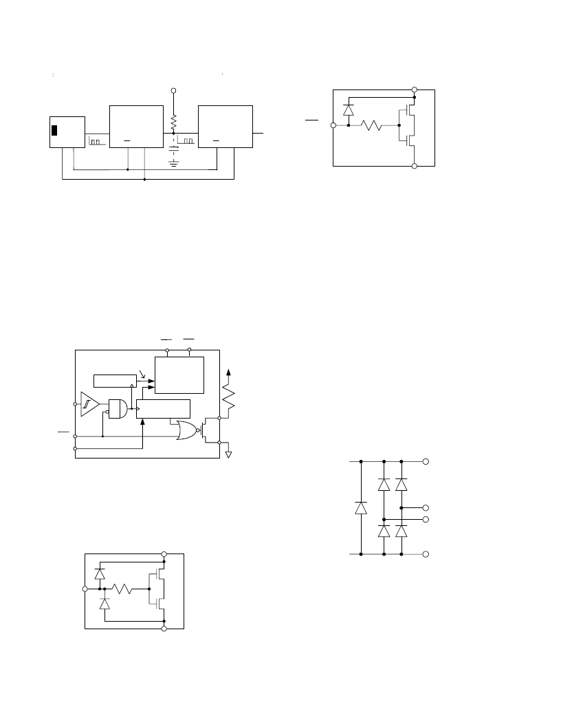
DIGITAL INPUT/OUTPUT CONFIGURATION
All digital inputs are ESD protected. Digital inputs are high
impedance and can be driven directly from most digital sources.
For
PR
and
WP
, which are active at logic low, should be biased
to V
DD
if they are not used. There are no internal pull-up
resistors on any digital input pin. As a result, pull-up resistors
are needed if these functions are used.
For SDO and RDY pins, they are open drain digital outputs.
Similarly, pull-up resistors are needed if these functions are
used. To optimize the speed and power trade off, use 2.2k
pull-up resistors.
SERIAL
REGISTER
COUNTER
COMMAND
PROCESSOR
& ADDRESS
DECODE
VALID
COMMAND
CS
SDI
CLK
R
PULLUP
+5V
SDO
GND
PR
WP
Figure 6. Equivalent Digital Input-Output Logic
The equivalent serial data input and output logic is shown in
figure 6. The open drain output SDO is disabled whenever chip
select
CS
is logic high. The SPI interface can be used in two
slave modes CPHA=1, CPOL=1 and CPHA=0, CPOL=0..
ESD protection of the digital inputs is shown in figures 7A &
7B.
INPUTS
LOGIC
PINS
V
DD
GND
300
Figure 7A. Equivalent ESD Digital Input Protection
INPUT
300
WP
V
DD
GND
Figure 7B. Equivalent
WP
Input Protection
SERIAL DATA INTERFACE
The ADN2850 contains a four-wire SPI compatible digital
interface (SDI, SDO, CS, and CLK). The 24-bit serial word
must be loaded with MSB first, and the format of the word is
shown in Table 1. The Command Bits (C0 to C3) control the
operation of the programmable resistor according to the
instruction shown in Table 2. A0 to A3 are assigned for address
bits. A0 is used to address RDAC 1 or RDAC2. Addresses 2 to
14 are accessable by users. Address 15 is reserved for factory
usage. Table 4 provides an address map of the EEMEM
locations. The Data Bits (D0 to D15) are the values that are
loaded into the RDAC register.
The last instruction prior to a period of no programming activity
should be applied with the No Operation (NOP), instruction 0. It
is recommended to do so to ensure minimum power
consumption in the internal logic circuitry
TERMINAL VOLTAGE OPERATING RANGE
The ADN2850 positive V
DD
and negative V
SS
power supply
defines the boundary conditions for proper 2-terminal
programmable resistance operation. Supply signals present on
terminals W and B that exceed V
DD
or V
SS
will be clamped by
the internal forward biased diodes, see Figure 8.
V
DD
W
B
V
SS
Figure 8. Maximum Terminal Voltages Set by V
DD
& V
SS
The ground pin of the ADN2850 device is primarily used as a
digital ground reference, which needs to be tied to the PCB's
common ground. The digital input contol signals to the
ADN2850 must be referenced to the device ground pin (GND),
and satisfy the logic level defined in the specification table of
this data sheet. An internal level shift circuit insures that the
common mode voltage range of the 2-terminals extends from
V
SS
to V
DD
irrespective of the digital input level.
相關(guān)PDF資料 |
PDF描述 |
|---|---|
| ADN2850ACP250-RL7 | Nonvolatile Memory, Dual 1024 Position Programmable Resistors |
| ADN2860 | High Bandwidth, CMOS 8-Bit Serial Interface Multiplying D/A Converter; Package: MSOP; No of Pins: 10; Temperature Range: Industrial |
| ADN2870 | High Bandwidth, CMOS 8-Bit Serial Interface Multiplying D/A Converter; Package: MSOP; No of Pins: 10; Temperature Range: Industrial |
| ADN2870ACPZ | High Bandwidth, CMOS 8-Bit Serial Interface Multiplying D/A Converter; Package: MSOP; No of Pins: 10; Temperature Range: Industrial |
| ADN2870ACPZ-RL | 3.3 V Dual-Loop, 50 Mbps to 3.3 Gbps Laser Diode Driver |
相關(guān)代理商/技術(shù)參數(shù) |
參數(shù)描述 |
|---|---|
| ADN2850ACP250-RL7 | 制造商:AD 制造商全稱:Analog Devices 功能描述:Nonvolatile Memory, Dual 1024 Position Programmable Resistors |
| ADN2850ACP25-RL7 | 制造商:AD 制造商全稱:Analog Devices 功能描述:Nonvolatile Memory, Dual 1024 Position Programmable Resistors |
| ADN2850ARU | 制造商:Analog Devices 功能描述:DUAL 10-BIT PROGRAMMABLE NON-VOLATILE RESISTOR - Bulk |
| ADN2850ARU25 | 制造商:AD 制造商全稱:Analog Devices 功能描述:Nonvolatile Memory, Dual 1024 Position Programmable Resistors |
| ADN2850ARU25-REEL7 | 制造商:AD 制造商全稱:Analog Devices 功能描述:Nonvolatile Memory, Dual 1024 Position Programmable Resistors |
發(fā)布緊急采購(gòu),3分鐘左右您將得到回復(fù)。