- 您現在的位置:買賣IC網 > PDF目錄374017 > ADN8830 (Analog Devices, Inc.) Thermoelectric Cooler Controller PDF資料下載
參數資料
| 型號: | ADN8830 |
| 廠商: | Analog Devices, Inc. |
| 英文描述: | Thermoelectric Cooler Controller |
| 中文描述: | 熱電冷卻器控制器 |
| 文件頁數: | 10/24頁 |
| 文件大小: | 416K |
| 代理商: | ADN8830 |
REV. C
–10–
ADN8830
To eliminate the resolution of the DAC as the principal source
of system error, the step size of each bit,
V
STEP
,
should be lower
than the desired system resolution. A practical value for absolute
DAC resolution is the equivalent of 0.05
°
C. The value of
V
STEP
should be less than the value of
m
from Equation 8 multiplied
by the desired temperature resolution, or
°
×
0 05
.
where
m
is the slope of the voltage-to-temperature conversion
line, as found from Equation 8. From Design Example 2, where
m
= 25 mV/
°
C, we see the DAC should have resolution better
than 1.25 mV per step.
The minimum number of bits required is then given as
(
log 2
V
C
m
STEP
<
(10)
Number of Bits
V
V
(
FS
STEP
=
)
)
log
–
log
(11)
where
V
FS
is the full-scale output voltage from the DAC, which
should be equal to the reference voltage from the ADN8830,
VREF = 2.47 V as given in the Specifications table for the
Reference Voltage. In this example, the minimum resolution is
11 bits. A 12-bit DAC, such as the AD7390, can be readily
found.
It is important that the full-scale voltage input to the DAC is tied
to the ADN8830 reference voltage, as shown in Figure 4. This
eliminates errors from slight variances of VREF.
Thermistor Fault and Temperature Lock Indications
Both the THERMFAULT (Pin 1) and TEMPLOCK (Pin 5)
outputs are CMOS compatible outputs that are active high.
THERMFAULT will be a logic low while the thermistor is
operating normally and will go to a logic high if a short or
open is detected at THERMIN (Pin 2). The trip voltage for
THERMFAULT is when THERMIN falls below 0.2 V or
exceeds 2.0 V. THERMFAULT provides only an indication of
a fault condition and does not activate any shutdown or protec-
tion circuitry on the ADN8830. To shut down the ADN8830, a
logic low voltage must be asserted on Pin 3, as described in the
Shutdown Mode section.
TEMPLOCK will output a logic high when the voltage at
THERMIN is within 2.5 mV of TEMPSET. This voltage can
be related to temperature by solving for
m
from Equation 8. For
most laser diode applications, 2.5 mV is equivalent to
±
0.1
°
C.
If the voltage difference between THERMIN and TEMPSET is
greater than 2.5 mV, then TEMPLOCK will output a logic low.
The input offset voltage of the ADN8830 is guaranteed to within
250
μ
V, which for most applications is within
±
0.01
°
C.
Setting the Switching Frequency
The ADN8830 has an internal oscillator to generate the switch-
ing frequency for the output stage. This oscillator can be either
set in free-run mode or synchronized to an external clock
signal. For free-run operation, SYNCIN (Pin 25) should be
connected to ground and COMPOSC (Pin 24) should be
connected to AVDD. The switching frequency is then set by a
single resistor connected from FREQ (Pin 26) to ground.
Table I shows R
FREQ
for some common switching frequencies.
Table I. Switching Frequencies vs. R
FREQ
f
SWITCH
100 kHz
250 kHz
500 kHz
750 kHz
1 MHz
R
FREQ
1.5 M
600 k
300 k
200 k
150 k
For other frequencies, the value for this resistor,
R
FREQ
, should
be set to
R
f
FREQ
SWITCH
=
×
150
10
9
(12)
where
f
SWITCH
is the switching frequency in Hz.
Higher switching frequencies reduce the voltage ripple across
the TEC. However, high switch frequencies will create more
power dissipation in the external transistors. This is due to the
more frequent charging and discharging of the transistors
’
gate
capacitances. If large transistors are needed for a high output
current application, faster switching frequencies could reduce
the overall power efficiency of the circuit. This is covered in
detail in the Calculating Power Dissipation and Efficiency section.
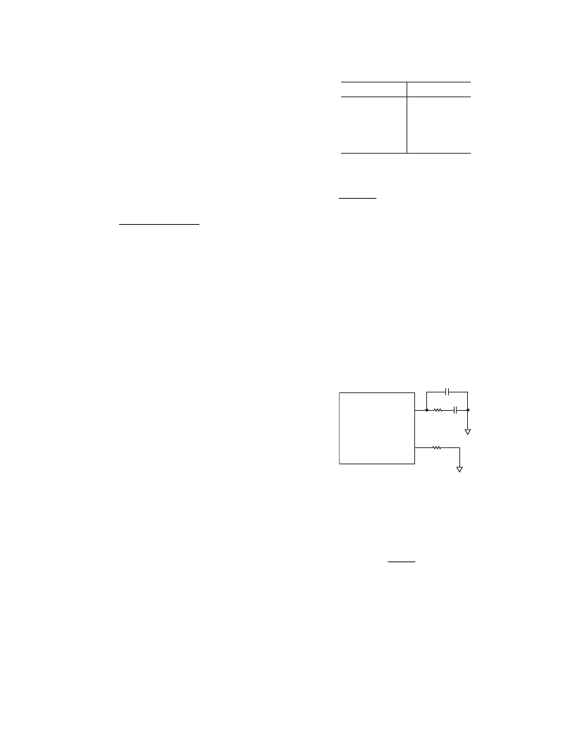
The switching frequency of the ADN8830 can be synchronized
with an external clock by connecting the clock signal to SYNCIN
(Pin 25). Pin 24 should also be connected to an R-C network, as
shown in Figure 6. This network is simply used to compensate a
PLL to lock on to the external clock. To ensure the quickest
synchronization lock-in time, R
FREQ
should be set to 1.5 M
.
ADN8830
FREQ
COMPOSC
1.5M
26
24
0.1 F
1k
1nF
Figure 6. Using an R-C Network on Pin 24 with
an External Clock
The relative phase of the ADN8830 internal oscillator compared
to the external clock signal can be adjusted. This is accomplished
by adjusting the voltage to PHASE (Pin 29) according to TPCs 3
and 4. The phase shift versus voltage can be approximated as
Phase Shift
where
V
PHASE
is the voltage at Pin 29, and
VREF
has a typical
value of 2.47 V.
To ensure the oscillator operates correctly,
V
PHASE
should remain
higher than 100 mV and lower than 2.3 V. This is required for
either internal clock or external synchronization operation. A
resistor divider from
VREF
to ground can establish this voltage
easily, although any voltage source, such as a DAC, could be used
as well. If phase is not a consideration, for example with a single
ADN8830 being used, Pin 29 can be tied to Pin 6, which pro-
vides a 1.5 V reference voltage.
V
VREF
PHASE
° =
° ×
360
(13)
相關PDF資料 |
PDF描述 |
|---|---|
| ADN8831 | Thermoelectric Cooler (TEC) Controller |
| ADP1073 | Circular Connector; MIL SPEC:MIL-DTL-38999 Series I; Body Material:Metal; Series:LJT; No. of Contacts:100; Connector Shell Size:23; Connecting Termination:Crimp; Circular Shell Style:Straight Plug; Body Style:Straight RoHS Compliant: No |
| ADP1073AN | Circular Connector; No. of Contacts:100; Series:LJT06R; Body Material:Aluminum; Connecting Termination:Crimp; Connector Shell Size:23; Circular Contact Gender:Pin; Circular Shell Style:Straight Plug; Insert Arrangement:23-35 |
| ADP1073AN-12 | Circular Connector; MIL SPEC:MIL-DTL-38999 Series I; Body Material:Metal; Series:LJT; No. of Contacts:100; Connector Shell Size:23; Connecting Termination:Crimp; Circular Shell Style:Straight Plug; Body Style:Straight RoHS Compliant: No |
| ADP1073AN-33 | Circular Connector; No. of Contacts:100; Series:LJT06R; Body Material:Aluminum; Connecting Termination:Crimp; Connector Shell Size:23; Circular Contact Gender:Socket; Circular Shell Style:Straight Plug; Insert Arrangement:23-35 |
相關代理商/技術參數 |
參數描述 |
|---|---|
| ADN8830ACP | 制造商:Analog Devices 功能描述:Temp Sensor Digital 32-Pin LFCSP EP 制造商:Rochester Electronics LLC 功能描述:HIGH PRECISION/EFFICIENCY TEC CONTROLLER - Bulk |
| ADN8830ACP-REEL | 制造商:Analog Devices 功能描述:Temp Sensor Digital 32-Pin LFCSP EP T/R |
| ADN8830ACP-REEL7 | 制造商:Rochester Electronics LLC 功能描述: 制造商:Analog Devices 功能描述: |
| ADN8830ACP-WP | 制造商:Analog Devices 功能描述:HIGH PRECISION/EFFICIENCY TEC CONTROLLER - Trays |
| ADN8830ACPZ | 功能描述:IC CTRLR THERMO COOLER 32-LFCSP RoHS:是 類別:集成電路 (IC) >> PMIC - 電源管理 - 專用 系列:- 產品培訓模塊:Lead (SnPb) Finish for COTS Obsolescence Mitigation Program 標準包裝:50 系列:- 應用:熱電冷卻器 電流 - 電源:- 電源電壓:3 V ~ 5.5 V 工作溫度:-40°C ~ 85°C 安裝類型:表面貼裝 封裝/外殼:28-SOIC(0.173",4.40mm 寬)裸露焊盤 供應商設備封裝:28-TSSOP 裸露焊盤 包裝:管件 產品目錄頁面:1410 (CN2011-ZH PDF) |
發布緊急采購,3分鐘左右您將得到回復。