- 您現在的位置:買賣IC網 > Datasheet目錄39 > ADP2140ACPZ3328R7 (Analog Devices Inc)IC REG DL BCK/LINEAR 10LFCSP Datasheet資料下載
參數資料
| 型號: | ADP2140ACPZ3328R7 |
| 廠商: | Analog Devices Inc |
| 文件頁數: | 21/32頁 |
| 文件大小: | 2731K |
| 描述: | IC REG DL BCK/LINEAR 10LFCSP |
| 標準包裝: | 1 |
| 拓撲: | 降壓(降壓)同步(1),線性(LDO)(1) |
| 功能: | 任何功能 |
| 輸出數: | 2 |
| 頻率 - 開關: | 3MHz |
| 電壓/電流 - 輸出 1: | 3.3V,600mA |
| 電壓/電流 - 輸出 2: | 2.8V,300mA |
| 帶 LED 驅動器: | 無 |
| 帶監控器: | 無 |
| 帶序列發生器: | 是 |
| 電源電壓: | 1.65 V ~ 5.5 V |
| 工作溫度: | -40°C ~ 125°C |
| 安裝類型: | 表面貼裝 |
| 封裝/外殼: | 10-WFDFN 裸露焊盤,CSP |
| 供應商設備封裝: | 10-LFCSP-WD(3x3) |
| 包裝: | 標準包裝 |
| 其它名稱: | ADP2140ACPZ3328R7DKR |
第1頁第2頁第3頁第4頁第5頁第6頁第7頁第8頁第9頁第10頁第11頁第12頁第13頁第14頁第15頁第16頁第17頁第18頁第19頁第20頁當前第21頁第22頁第23頁第24頁第25頁第26頁第27頁第28頁第29頁第30頁第31頁第32頁
Data Sheet
ADP2140
Rev. A | Page 21 of 32
APPLICATIONS INFORMATION
POWER SEQUENCING
The ADP2140 has a flexible power sequencing system
supporting two distinct activation modes:
? Individual activation control is where EN1 controls only
the buck regulator and EN2 controls only the LDO. A high
level on Pin EN1 turns on the buck and a high level on
Pin EN2 turns on the LDO. A logic low level turns off the
respective regulator.
? Autosequencing is where the two regulators turn on in a
specified order and delay after a low-to-high transition on
the EN1 pin.
Select the activation mode (individual or autosequence) by
decoding the state of Pin EN2. The individual activation mode
is selected when the EN2 pin is driven externally or hardwired
to a voltage level (VIN1 or PGND). The autosequencing mode
is selected when the EN2 pin remains unconnected (floating).
To minimize quiescent current consumption, the mode selection
executes one time only during the rising edge of VIN1. The
detection circuit then activates for the time needed to assess the
EN2 state, after which time the circuit is disabled until VIN1 falls
below 0.5 V .
When EN2 is unconnected, the internal control circuit provides
a termination resistance to ground. The 100 k?termination
resistance is low enough to guarantee insensitivity to noise and
transients. The termination resistor is disabled in the event that
the EN2 pin is driven externally to a logic level high (individual
activation mode assumed) to reduce the quiescent current con-
sumption.
When the autosequencing mode is selected, the EN1 pin is used to
start the on/off sequence of the regulators. A logic high sequences
the regulators on whereas a logic low sequences the regulators
off. The regulator activation order is associated with the voltage
selected for the buck regulator and the LDO.
When the turn on or turn off autosequence starts, the start-up
delay between the first and the second regulator is fixed to 5 ms
in PWM mode (tREG12, as shown in Figure 71 and Figure 72).
When the application requires activating and deactivating the
regulators at the same time, use the individual activation mode,
which connects the EN1 and EN2 pins together, as shown in
Figure 75.
Table 6. Power Sequencing Modes
EN2
1
EN1
Description
0
0
Individual mode: both regulators are off.
0
1
Individual mode: buck regulator is on.
1
0
Individual mode: LDO regulator is on.
1
1
Individual mode: both regulators are on.
NC
Rising edge Autosequence: Buck regulator turns on,
then the LDO regulator turns on. The LDO
voltage is less than the buck voltage.
NC
Rising edge Autosequence: LDO regulator turns on,
then the buck regulator turns on. The LDO
voltage is greater than the buck voltage.
NC
Rising edge Autosequence: If the buck voltage is 1.875 V,
then the LDO regulator always turns on first.
NC
Falling edge Autosequence: The LDO and buck regula-
tors turn off at the same time.
1
NC means not connected.
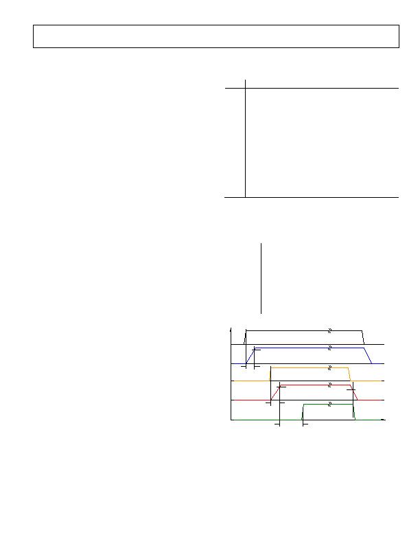
Figure 70 to Figure 75 use the following symbols, as described in
Table 7.
Table 7. Timing Symbols
Symbol
Description
Typical
Value
t
START
Time needed for the internal circuitry
to activate the first regulator
60 約
t
SS
Regulator soft start time
330 約
tRESET
Time delay from power-good
condition to the release of PG
5 ms
t
REG12
Delay time between buck and LDO
activation
5 ms
EN1
V
BUCK
EN2
V
LDO
PG
92% V
BUCK
92% V
LDO
85% V
LDO
t
SS
t
RESET
t
SS
TIME
Figure 70. Individual Activation Mode
相關PDF資料 |
PDF描述 |
|---|---|
| ADP5022ACBZ-6-R7 | IC REG TRPL BCK/LINEAR 16WLCSP |
| ADP5041ACPZ-1-R7 | IC REG TRPL BCK/LINEAR 20-LFCSP |
| ADP5042ACPZ-2-R7 | IC REG TRPL BCK/LINEAR 20LFCSP |
| ADT6402SRJZ-RL7 | IC TEMP SENS TRIP PT PP SOT-23-6 |
| ADT6501SRJZP085RL7 | IC TEMP SENSOR MICROPWR SOT23-5 |
相關代理商/技術參數 |
參數描述 |
|---|---|
| ADP2140CPZ-REDYKIT | 功能描述:REDYKIT 2 BOARDS ADP2140ACPZ RoHS:是 類別:編程器,開發系統 >> 評估板 - 線性穩壓器 (LDO) 系列:* 產品變化通告:1Q2012 Discontinuation 30/Mar/2012 設計資源:NCP590MNDPTAGEVB Gerber Files 標準包裝:1 系列:- 每 IC 通道數:2 - 雙 輸出電壓:1.8V,2.8V 電流 - 輸出:300mA 輸入電壓:2.1 ~ 5.5 V 穩壓器類型:正,固定式 工作溫度:-40°C ~ 85°C 板類型:完全填充 已供物品:板 已用 IC / 零件:NCP590MNDP 其它名稱:NCP590MNDPTAGEVB-NDNCP590MNDPTAGEVBOS |
| ADP2147 | 制造商:AD 制造商全稱:Analog Devices 功能描述:Compact, 800 mA, 3 MHz, Simple DVS, Buck Regulator Input voltage: 2.3 V to 5.5 V |
| ADP2147ACBZ-110-R7 | 功能描述:IC REG BUCK SYNC 0.8A 6WLCSP RoHS:是 類別:集成電路 (IC) >> PMIC - 穩壓器 - DC DC 開關穩壓器 系列:- 產品培訓模塊:High Efficiency Current Mode Switching Regulators CMOS LDO Regulators 特色產品:BD91x Series Step-Down Regulators 標準包裝:2,500 系列:- 類型:降壓(降壓) 輸出類型:兩者兼有 輸出數:2 輸出電壓:3.3V,0.8 V ~ 2.5 V 輸入電壓:4.5 V ~ 5.5 V PWM 型:電流模式 頻率 - 開關:1MHz 電流 - 輸出:1.5A 同步整流器:是 工作溫度:-40°C ~ 85°C 安裝類型:表面貼裝 封裝/外殼:20-VFQFN 裸露焊盤 包裝:帶卷 (TR) 供應商設備封裝:VQFN020V4040 產品目錄頁面:1373 (CN2011-ZH PDF) 其它名稱:BD9152MUV-E2TR |
| ADP2147ACBZ-130-R7 | 功能描述:IC REG BUCK SYNC 0.8A 6WLCSP RoHS:是 類別:集成電路 (IC) >> PMIC - 穩壓器 - DC DC 開關穩壓器 系列:- 標準包裝:500 系列:- 類型:切換式電容器(充電泵),反相 輸出類型:固定 輸出數:1 輸出電壓:-3V 輸入電壓:2.3 V ~ 5.5 V PWM 型:Burst Mode? 頻率 - 開關:900kHz 電流 - 輸出:100mA 同步整流器:無 工作溫度:-40°C ~ 85°C 安裝類型:表面貼裝 封裝/外殼:SOT-23-6 細型,TSOT-23-6 包裝:帶卷 (TR) 供應商設備封裝:TSOT-23-6 其它名稱:LTC1983ES6-3#TRMTR |
| ADP2147ACBZ-150-R7 | 功能描述:IC REG BUCK SYNC 1.2V/1V 6WLCSP RoHS:是 類別:集成電路 (IC) >> PMIC - 穩壓器 - DC DC 開關穩壓器 系列:- 標準包裝:500 系列:- 類型:切換式電容器(充電泵),反相 輸出類型:固定 輸出數:1 輸出電壓:-3V 輸入電壓:2.3 V ~ 5.5 V PWM 型:Burst Mode? 頻率 - 開關:900kHz 電流 - 輸出:100mA 同步整流器:無 工作溫度:-40°C ~ 85°C 安裝類型:表面貼裝 封裝/外殼:SOT-23-6 細型,TSOT-23-6 包裝:帶卷 (TR) 供應商設備封裝:TSOT-23-6 其它名稱:LTC1983ES6-3#TRMTR |
發布緊急采購,3分鐘左右您將得到回復。