- 您現(xiàn)在的位置:買賣IC網(wǎng) > PDF目錄374019 > ADP3050AR (ANALOG DEVICES INC) 200 kHz, 1 A High-Voltage Step-Down Switching Regulator PDF資料下載
參數(shù)資料
| 型號(hào): | ADP3050AR |
| 廠商: | ANALOG DEVICES INC |
| 元件分類: | 穩(wěn)壓器 |
| 英文描述: | 200 kHz, 1 A High-Voltage Step-Down Switching Regulator |
| 中文描述: | 2.1 A SWITCHING REGULATOR, 240 kHz SWITCHING FREQ-MAX, PDSO8 |
| 封裝: | MS-012AA, SOIC-8 |
| 文件頁(yè)數(shù): | 15/16頁(yè) |
| 文件大小: | 191K |
| 代理商: | ADP3050AR |
第1頁(yè)第2頁(yè)第3頁(yè)第4頁(yè)第5頁(yè)第6頁(yè)第7頁(yè)第8頁(yè)第9頁(yè)第10頁(yè)第11頁(yè)第12頁(yè)第13頁(yè)第14頁(yè)當(dāng)前第15頁(yè)第16頁(yè)
ADP3050
–
15
–
REV. 0
R2
R1
CC
RC
OUTPUT
GROUND
INPUT
C1
L1
C3
D1
D2
C2
ADP3050
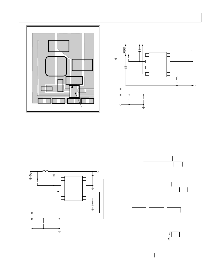
Figure 25. Recommended Board Layout
TYPICAL APPLICATIONS
5 V to 3.3 V Buck (Step-Down) Regulator
The circuit in Figure 26 shows the ADP3050 in a buck configu-
ration. It is used to generate 3.3 V regulated output from 5 V
input voltage with the following specifications:
V
IN
= 4.5 V to 5.5 V
V
OUT
= 3.3 V
I
OUT
= 0.75 A
I
RIPPLE
= 0.4 A 0.75 A = 0.3 A
V
OUT RIPPLE
= 50 mV
U1
ADP3050-3.3
V
IN
1
2
3
4
SWITCH
BOOST
BIAS
FB
IN
GND
SD
COMP
8
7
6
5
C3
0.22 F
D1
1N5817
GND
5V
C1
22 F
+
C2
0.01 F
L1
22 H
V
OUT
3.3V
R1
7.5k
C4
1nF
D2
1N4148
+C5
100 F
SD
Figure 26. 5 V to 3.3 V Buck Regulator
INVERTING (BUCK-BOOST) REGULATOR
The circuit in Figure 27 shows the ADP3050 in a buck-boost
configuration, which produces a negative output voltage from a
positive input voltage. This topology looks quite similar to the
buck shown in Figure 26 above (except the IC and the output
filter are now referenced to the negative output instead of
ground), but its operation is quite different. For this topology,
the feedback pin is grounded and the GND pin is tied to the
negative output, allowing the feedback network of the IC to
regulate the negative output voltage.
U1
ADP3050-5
V
IN
1
2
3
4
SWITCH
BOOST
BIAS
FB
IN
GND
SD
COMP
8
7
6
5
C3
0.22 F
D1
1N5818
GND
12V
C1
22 F
+
C2
0.01 F
R1
5.1k
C4
3.3nF
D2
1N4148
+
C5
100 F
SD
5V @ 0.5A
V
OUT
L1
47 H
NC
Figure 27. Inverting (Buck-Boost) Regulator
The design procedure used for the standard buck converter cannot
be used for a buck-boost converter due to fundamental differences
in how the output voltage is generated. The switch currents in the
buck-boost are much higher than in the standard buck converter,
thus lowering the available load current. To calculate the maximum
output current for a given maximum switch current use the following
equation:
I
V
+
V
V
I
V
×
V
(
f
L
V
V
OUT
IN
IN
OUT
SW
IN
OUT
SW
IN
OUT
(MAX)
(MAX)
=
×
×
×
×
+
)
2
(15)
where I
SW(MAX)
is the switch current limit rating of the ADP3050
and
V
IN
is the minimum input voltage. The inductor ripple current
can be estimated using the following equation:
I
V
L
f
V
V
V
RIPPLE
IN
SW
OUT
IN
OUT
=
×
×
+
(MAX)
(MAX)
1
(16)
For the circuit in Figure 27, the maximum ripple current (at the
maximum input voltage) is:
I
A
RIPPLE
=
×
×
×
×
+
=
12
47
10
1
200
10
5
12
5
0.
6
3
High ripple currents are present in both the input and output
capacitors, and their ripple current ratings must be large enough
to sustain the large switching currents present in this topology.
The capacitors should have a ripple current rating of at least:
I
I
V
V
RMS
OUT
OUT
IN
(CIN, COUT)
≈
×
(17)
The peak current seen by the diode, switch, and inductor can be
found by rearranging the load current equation:
I
V
V
V
I
I
PEAK
IN
OUT
IN
OUT
RIPPLE
=
+
×
+
×
1
2
(18)
相關(guān)PDF資料 |
PDF描述 |
|---|---|
| ADP3155 | 5-Bit Programmable Triple Power Supply Controller for Pentium III Processors |
| ADP3155JRU | 5-Bit Programmable Triple Power Supply Controller for Pentium III Processors |
| ADP3156JR-15 | Dual Power Supply Controller for Desktop Systems |
| ADP3156JR-18 | Dual Power Supply Controller for Desktop Systems |
| ADP3156JR-25 | Dual Power Supply Controller for Desktop Systems |
相關(guān)代理商/技術(shù)參數(shù) |
參數(shù)描述 |
|---|---|
| ADP3050AR3.3 | 制造商:Analog Devices 功能描述:IC ((NS)) |
| ADP3050AR-3.3 | 功能描述:IC REG BUCK 3.3V 1A 8SOIC RoHS:否 類別:集成電路 (IC) >> PMIC - 穩(wěn)壓器 - DC DC 開(kāi)關(guān)穩(wěn)壓器 系列:- 設(shè)計(jì)資源:Design Support Tool 標(biāo)準(zhǔn)包裝:1 系列:- 類型:升壓(升壓) 輸出類型:固定 輸出數(shù):1 輸出電壓:3V 輸入電壓:0.75 V ~ 2 V PWM 型:- 頻率 - 開(kāi)關(guān):- 電流 - 輸出:100mA 同步整流器:是 工作溫度:-40°C ~ 85°C 安裝類型:表面貼裝 封裝/外殼:SOT-23-5 細(xì)型,TSOT-23-5 包裝:剪切帶 (CT) 供應(yīng)商設(shè)備封裝:TSOT-23-5 其它名稱:AS1323-BTTT-30CT |
| ADP3050AR-3.3-REEL | 制造商:Analog Devices 功能描述:Conv DC-DC Single Step Down 3.6V to 30V 8-Pin SOIC N T/R |
| ADP3050AR-3.3-RL7 | 功能描述:IC REG BUCK 3.3V 1A 8SOIC RoHS:否 類別:集成電路 (IC) >> PMIC - 穩(wěn)壓器 - DC DC 開(kāi)關(guān)穩(wěn)壓器 系列:- 標(biāo)準(zhǔn)包裝:2,500 系列:- 類型:升壓(升壓) 輸出類型:可調(diào)式 輸出數(shù):1 輸出電壓:1.24 V ~ 30 V 輸入電壓:1.5 V ~ 12 V PWM 型:電流模式,混合 頻率 - 開(kāi)關(guān):600kHz 電流 - 輸出:500mA 同步整流器:無(wú) 工作溫度:-40°C ~ 85°C 安裝類型:表面貼裝 封裝/外殼:8-SOIC(0.154",3.90mm 寬) 包裝:帶卷 (TR) 供應(yīng)商設(shè)備封裝:8-SOIC |
| ADP3050AR-33 | 制造商:AD 制造商全稱:Analog Devices 功能描述:200 kHz, 1 A High-Voltage Step-Down Switching Regulator |
發(fā)布緊急采購(gòu),3分鐘左右您將得到回復(fù)。