- 您現在的位置:買賣IC網 > PDF目錄374019 > ADP3050AR (ANALOG DEVICES INC) 200 kHz, 1 A High-Voltage Step-Down Switching Regulator PDF資料下載
參數資料
| 型號: | ADP3050AR |
| 廠商: | ANALOG DEVICES INC |
| 元件分類: | 穩壓器 |
| 英文描述: | 200 kHz, 1 A High-Voltage Step-Down Switching Regulator |
| 中文描述: | 2.1 A SWITCHING REGULATOR, 240 kHz SWITCHING FREQ-MAX, PDSO8 |
| 封裝: | MS-012AA, SOIC-8 |
| 文件頁數: | 3/16頁 |
| 文件大小: | 191K |
| 代理商: | ADP3050AR |
ADP3050
–3–
REV. 0
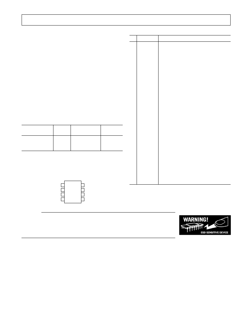
PIN FUNCTION DESCRIPTION
Pin
Name
Function
1
SWITCH
This is the emitter of the internal NPN
power switch. The voltage at this pin switches
between V
IN
and approximately –0.5 V.
This pin is used to provide a boosted voltage
(higher than V
IN
) for the drive stage of the
NPN power switch. With the higher drive
voltage, the power switch can be saturated,
greatly reducing the switch power losses.
Connect this pin to the regulated output
voltage to maximize system efficiency.
When this pin is above 2.7 V, most of the
ADP3050 operating current will be taken
from the output instead of the input supply.
Leave unconnected if not used.
This feedback pin senses the regulated output
voltage. Connect this pin directly to the out-
put (fixed output versions).
This pin is used to compensate the regulator
with an external resistor and capacitor. This
pin can be used to override the control loop,
but the voltage on this pin should not exceed
about 2 V, as the pin is internally clamped to
ensure a fast transient response. Use a pull-up
resistor if this pin is to be pulled higher than 2 V.
Use this pin to turn the device on and off. If
this feature is not needed, tie this pin directly
to V
IN
.
Connect this pin to local ground plane.
Connect this pin to the input supply voltage.
An input bypass capacitor must be placed
close to this pin to ensure proper regulator
operation.
2
BOOST
3
BIAS
4
FB
5
COMP
6
SD
7
8
GND
IN
ABSOLUTE MAXIMUM RATINGS
*
IN Voltage
Steady State . . . . . . . . . . . . . . . . . . . . . . . . –0.3 V to +30 V
Peak (<100 ms) . . . . . . . . . . . . . . . . . . . . . –0.3 V to +60 V
BOOST Voltage
Steady State . . . . . . . . . . . . . . . . . . . . . . . . –0.3 V to +45 V
Peak (<100 ms) . . . . . . . . . . . . . . . . . . . . . –0.3 V to +65 V
SD
, BIAS Voltage . . . . . . . . . . . . . . . . . –0.3 V to IN + 0.3 V
FB Voltage . . . . . . . . . . . . . . . . . . . . . . . . . . . . –0.3 V to +8 V
COMP Voltage . . . . . . . . . . . . . . . . . . . –0.3 V to IN + 0.3 V
SWITCH Voltage . . . . . . . . . . . . . . . . . –0.3 V to IN + 0.3 V
Operating Ambient Temperature Range . . . . –40
°
C to +85
°
C
Operating Junction Temperature Range . . . –40
°
C to +125
°
C
Storage Temperature Range . . . . . . . . . . . . –65
°
C to +150
°
C
θ
JA
(2-Layer PCB) . . . . . . . . . . . . . . . . . . . . . . . . . . 108
°
C/W
θ
JA
(4-Layer PCB) . . . . . . . . . . . . . . . . . . . . . . . . . . . 81
°
C/W
Lead Temperature Range (Soldering, 60 sec.) . . . . . . . . 300
°
C
*
This is a stress rating only; operation beyond these limits can cause the device to
be permanently damaged. Unless otherwise specified, all voltages are referenced
to GND
ORDERING GUIDE
PIN CONFIGURATION
8-Lead SOIC
(R-Suffix)
TOP VIEW
(Not to Scale)
8
7
6
5
1
2
3
4
SWITCH
BOOST
BIAS
FB
IN
GND
SD
COMP
ADP3050
Output
Voltage
Temperature
Range
–40
°
C to +85
°
C
–40
°
C to +85
°
C
–40
°
C to +85
°
C
Model
Package
*
ADP3050AR
ADP3050AR-3.3
ADP3050AR-5
ADJ
3.3 V
5.0 V
SO-8
SO-8
SO-8
*
SO = Small Outline Package
CAUTION
ESD (electrostatic discharge) sensitive device. Electrostatic charges as high as 4000 V readily
accumulate on the human body and test equipment and can discharge without detection.
Although this device features proprietary ESD protection circuitry, permanent damage may occur
on devices subjected to high energy electrostatic discharges. Therefore, proper ESD
precautions are recommended to avoid performance degradation or loss of functionality.
相關PDF資料 |
PDF描述 |
|---|---|
| ADP3155 | 5-Bit Programmable Triple Power Supply Controller for Pentium III Processors |
| ADP3155JRU | 5-Bit Programmable Triple Power Supply Controller for Pentium III Processors |
| ADP3156JR-15 | Dual Power Supply Controller for Desktop Systems |
| ADP3156JR-18 | Dual Power Supply Controller for Desktop Systems |
| ADP3156JR-25 | Dual Power Supply Controller for Desktop Systems |
相關代理商/技術參數 |
參數描述 |
|---|---|
| ADP3050AR3.3 | 制造商:Analog Devices 功能描述:IC ((NS)) |
| ADP3050AR-3.3 | 功能描述:IC REG BUCK 3.3V 1A 8SOIC RoHS:否 類別:集成電路 (IC) >> PMIC - 穩壓器 - DC DC 開關穩壓器 系列:- 設計資源:Design Support Tool 標準包裝:1 系列:- 類型:升壓(升壓) 輸出類型:固定 輸出數:1 輸出電壓:3V 輸入電壓:0.75 V ~ 2 V PWM 型:- 頻率 - 開關:- 電流 - 輸出:100mA 同步整流器:是 工作溫度:-40°C ~ 85°C 安裝類型:表面貼裝 封裝/外殼:SOT-23-5 細型,TSOT-23-5 包裝:剪切帶 (CT) 供應商設備封裝:TSOT-23-5 其它名稱:AS1323-BTTT-30CT |
| ADP3050AR-3.3-REEL | 制造商:Analog Devices 功能描述:Conv DC-DC Single Step Down 3.6V to 30V 8-Pin SOIC N T/R |
| ADP3050AR-3.3-RL7 | 功能描述:IC REG BUCK 3.3V 1A 8SOIC RoHS:否 類別:集成電路 (IC) >> PMIC - 穩壓器 - DC DC 開關穩壓器 系列:- 標準包裝:2,500 系列:- 類型:升壓(升壓) 輸出類型:可調式 輸出數:1 輸出電壓:1.24 V ~ 30 V 輸入電壓:1.5 V ~ 12 V PWM 型:電流模式,混合 頻率 - 開關:600kHz 電流 - 輸出:500mA 同步整流器:無 工作溫度:-40°C ~ 85°C 安裝類型:表面貼裝 封裝/外殼:8-SOIC(0.154",3.90mm 寬) 包裝:帶卷 (TR) 供應商設備封裝:8-SOIC |
| ADP3050AR-33 | 制造商:AD 制造商全稱:Analog Devices 功能描述:200 kHz, 1 A High-Voltage Step-Down Switching Regulator |
發布緊急采購,3分鐘左右您將得到回復。