- 您現在的位置:買賣IC網 > PDF目錄374019 > ADP3163 (Analog Devices, Inc.) 500-mA, 4.2-V Li-Ion Charger for Current-Limited App. w/Temp Sense in MSOP-8 8-MSOP-PowerPAD -40 to 85 PDF資料下載
參數資料
| 型號: | ADP3163 |
| 廠商: | Analog Devices, Inc. |
| 英文描述: | 500-mA, 4.2-V Li-Ion Charger for Current-Limited App. w/Temp Sense in MSOP-8 8-MSOP-PowerPAD -40 to 85 |
| 中文描述: | 5位可編程2-/3-Phase同步降壓控制器 |
| 文件頁數: | 4/16頁 |
| 文件大小: | 138K |
| 代理商: | ADP3163 |
REV. 0
ADP3163
–4–
PIN FUNCT ION DE SCRIPT IONS
Pin
Name
Function
1–5
VID4 –
VID0
Voltage Identification DAC Inputs. These pins are pulled up to an internal 3 V reference, providing a
Logic 1 if left open. The DAC output programs the FB regulation voltage from 1.1 V to 1.85 V. Leaving all five
DAC inputs open results in the ADP3163 going into a “No CPU” mode, shutting off its PWM outputs.
Current Sharing Output. This pin is connected to the SHARE pins of other ADP3163s in multiple VRM sys-
tems to ensure proper current sharing between the converters. The voltage at this output programs the output
current control level between CS+ and CS–.
Error Amplifier Output and Compensation Point.
Ground. FB, REF and the VID DAC of the ADP3163 are referenced to this ground. This is a low current ground
that can also be used as a return for the FB pin in remote voltage sensing applications.
Feedback Input. Error amplifier input for remote sensing of the output voltage.
External capacitor CT connection to ground sets the frequency of the device.
Open drain output that signals when the output voltage is outside of the proper operating range or when a phase
is not supplying current even if the output voltage is in specification.
Current Sense Positive Node. Positive input for the current comparator. The output current is sensed as a volt-
age at this pin with respect to CS–.
Current Sense Negative Node. Negative input for the current comparator.
Power Ground. All internal biasing and logic output signals of the ADP3163 are referenced to this ground.
Phase Control Input. This logic-level input determines the number of active phases and the duty cycle limit of
each phase.
Logic-Level Output for the Phase 3 Driver.
Logic-Level Output for the Phase 2 Driver.
Logic-Level Output for the Phase 1 Driver.
3.0 V Reference Output.
Supply Voltage for the ADP3163.
6
SHARE
7
8
COMP
GND
9
10
11
FB
CT
PWRGD
12
CS+
13
14
15
CS–
PGND
PC
16
17
18
19
20
PWM3
PWM2
PWM1
REF
VCC
5-BIT CODE
VID4
VID3
VID2
VID1
VID0
SHARE
COMP
GND
FB
CT
VCC
REF
PWM1
PWM2
PWM3
PC
PGND
CS
–
CS+
PWRGD
3
1
4
5
18
17
16
2
20
19
6
10
7
8
9
11
14
13
12
15
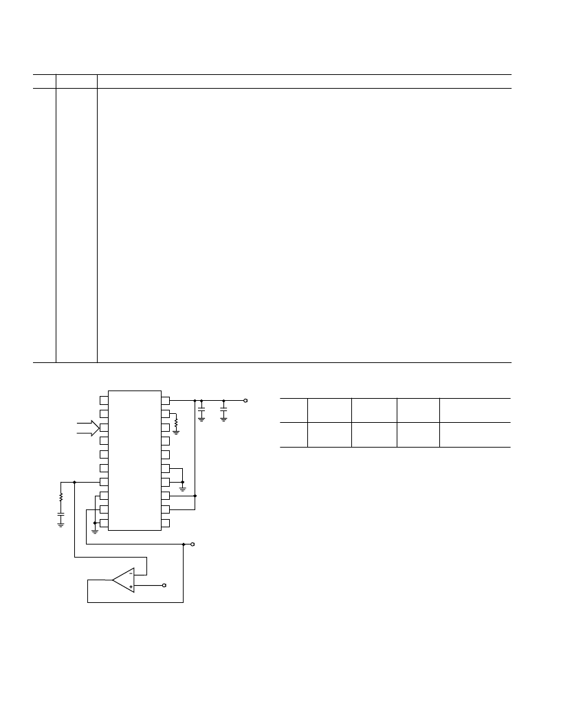
ADP3163
12V
100
100nF
1.2V
1 F
100nF
V
FB
20k
AD820
Figure 1. Closed-Loop Output Voltage Accuracy Test Circuit
T able I. PWM Outputs vs. Phase Control Code
Maximum
Duty Cycle
PC
PWM3
PWM2
PWM1
REF
GND
ON
OFF
ON
ON
ON
ON
33%
50%
相關PDF資料 |
PDF描述 |
|---|---|
| ADP3166 | 5-Bit Programmable 2-, 3-, 4-Phase Synchronous Buck Controller |
| ADP3166JRU-REEL | 5-Bit Programmable 2-, 3-, 4-Phase Synchronous Buck Controller |
| ADP3166JRU-REEL7 | 5-Bit Programmable 2-, 3-, 4-Phase Synchronous Buck Controller |
| ADP3170JRU | VRM 8.5 Compatible Single Phase Core Controller |
| ADP3170 | Charger front end protection IC with 30V max Vin and 4.5V LDO output 8-WSON 0 to 125 |
相關代理商/技術參數 |
參數描述 |
|---|---|
| ADP3163JRU | 制造商:AD 制造商全稱:Analog Devices 功能描述:5-Bit Programmable 2-/3-Phase Synchronous Buck Controller |
| ADP3163JRUZ-REEL | 功能描述:IC REG BUCK 5BIT 2-3PHAS 20TSSOP RoHS:是 類別:集成電路 (IC) >> PMIC - 穩壓器 - 專用型 系列:- 產品培訓模塊:Lead (SnPb) Finish for COTS Obsolescence Mitigation Program 標準包裝:2,000 系列:- 應用:電源,ICERA E400,E450 輸入電壓:4.1 V ~ 5.5 V 輸出數:10 輸出電壓:可編程 工作溫度:-40°C ~ 85°C 安裝類型:表面貼裝 封裝/外殼:42-WFBGA,WLCSP 供應商設備封裝:42-WLP 包裝:帶卷 (TR) |
| ADP3164 | 制造商:AD 制造商全稱:Analog Devices 功能描述:5-Bit Programmable 4-Phase Synchronous Buck Controller |
| ADP3164JRU | 制造商:AD 制造商全稱:Analog Devices 功能描述:5-Bit Programmable 4-Phase Synchronous Buck Controller |
| adp3164jruz-r7 | 制造商:ON Semiconductor 功能描述: |
發布緊急采購,3分鐘左右您將得到回復。