- 您現(xiàn)在的位置:買賣IC網(wǎng) > PDF目錄374019 > ADP3167JR (ANALOG DEVICES INC) 5-Bit Programmable 2-Phase Synchronous Buck Controller PDF資料下載
參數(shù)資料
| 型號: | ADP3167JR |
| 廠商: | ANALOG DEVICES INC |
| 元件分類: | 穩(wěn)壓器 |
| 英文描述: | 5-Bit Programmable 2-Phase Synchronous Buck Controller |
| 中文描述: | DUAL SWITCHING CONTROLLER, 2000 kHz SWITCHING FREQ-MAX, PDSO16 |
| 封裝: | SOIC-16 |
| 文件頁數(shù): | 8/16頁 |
| 文件大小: | 292K |
| 代理商: | ADP3167JR |
REV. B
–8–
ADP3160/ADP3167
C
T
Selection—Choosing the Clock Frequency
The ADP3160 and ADP3167 use a fixed-frequency control archi-
tecture. The frequency is set by an external timing capacitor, C
T
.
The value of C
T
for a given clock frequency can be selected using
the graph in Figure 2.
The clock frequency determines the switching frequency, which
relates directly to switching losses and the sizes of the inductors
and input and output capacitors. A clock frequency of 400 kHz
sets the switching frequency of each phase, f
SW
, to 200 kHz, which
represents a practical trade-off between the switching losses and
the sizes of the output filter components. From Figure 2, for 400 kHz
the required timing capacitor value is 150 pF. For good frequency
stability and initial accuracy, it is recommended to use a capacitor
with a low temperature coefficient and tight tolerance, e.g., an
MLC capacitor with NPO dielectric and with 5% or less tolerance.
Inductance Selection
The choice of inductance determines the ripple current in the
inductor. Less inductance leads to more ripple current, which
increases the output ripple voltage and the conduction losses in
the MOSFETs, but allows using smaller size inductors and, for
a specified peak-to-peak transient deviation, output capacitors
with less total capacitance. Conversely, a higher inductance
means lower ripple current and reduced conduction losses,
but requires larger size inductors and more output capacitance
for the same peak-to-peak transient deviation. In a 2-phase
converter a practical value for the peak-to-peak inductor ripple
current is under 50% of the dc current in the same inductor.
A choice of 46% for this particular design example yields a total
peak-to-peak output ripple current of 23% of the total dc output
current. The following equation shows the relationship between
the inductance, oscillator frequency, peak-to-peak ripple current
in an inductor, and input and output voltages.
L
V
(
V
V
V
f
I
IN
AVG
¥
AVG
IN
SW
L RIPPLE
(
=
¥
¥
–
)
)
(1)
For 12.5 A peak-to-peak ripple current, which corresponds to
just under 50% of the 26.7 A full-load dc current in an induc-
tor, Equation 1 yields an inductance of:
¥
¥
/
12
400
2 12 5
A 600 nH inductor can be used, which gives a calculated ripple
current of 12.2 A at no load. The inductor should not saturate
at the peak current of 32.8 A and should be able to handle the
sum of the power dissipation caused by the average current of
26.7 A in the winding and the core loss.
The output ripple current is smaller than the inductor ripple
current due to the two phases partially canceling. This can be
calculated as follows:
¥
¥
¥
12
600
400
Designing an Inductor
Once the inductance is known, the next step is either to design
an inductor or find a standard inductor that comes as close as
possible to meeting the overall design goals. The first decision in
designing the inductor is to choose the core material. There are
several possibilities for providing low core loss at high frequen-
cies. Two examples are the powder cores (e.g., Kool-M
m
from
Magnetics) and the gapped soft ferrite cores (e.g., 3F3 or 3F4
from Philips). Low-frequency powdered iron cores should be
avoided due to their high core loss, especially when the inductor
value is relatively low and the ripple current is high.
L
V
V
V
A
V
kHz
nH
=
=
(
–1 635
)
.
.
12
1 635
565
I
V
V
(
V
V
12
(
L
2 1 635
–
f
V
V
nH
V
V
kHz
A
O
AVG
IN
AVG
IN
OSC
.
D
=
¥
¥
=
¥
=
2
2
2 1 635
9 9
.
–
)
.
)
(2)
1
2
3
4
8
7
6
5
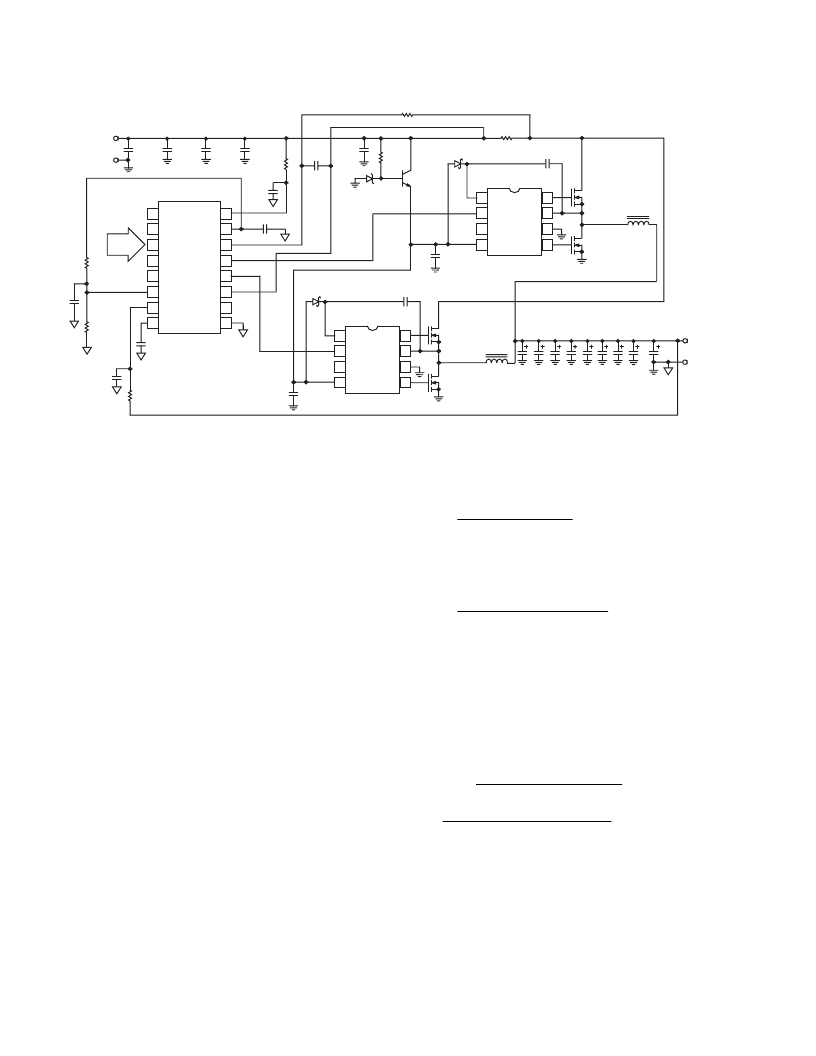
BST
IN
NC
VCC
DRVH
SW
PGND
DRVL
U2
ADP3414
U1
ADP3160
C23
C15C16 C17C18C19
270 F 4
OS-CON 16V
V
CC(CORE)
1.1V – 1.85V
53.4A
V
CC(CORE)
RTN
Q3
FDB7030L
D1
MBR052LTI
Q5
2N3904
L2
600nH
L1
600nH
Q1
FDB7030L
Q2
FDB8030L
C10
1 F
D2
MBR052LTI
C5
1 F
Z1
ZMM5236BCT
R5
2.4k
C25 1nF
C4
4.7 F
R6
10
C23
15nF
C14
C13
C12
C11
V
IN
12V
V
IN
RTN
C26
4.7 F
R
A
26.1k
C6
1 F
C9
1 F
R7
20
R4
4m
R
B
11.0k
C2
100pF
C1
150pF
R1
1k
Q4
FDB8030L
16
15
14
13
12
11
10
9
1
2
3
4
5
6
7
8
VID4
VID3
VID2
VID1
VID0
COMP
FB
CT
VCC
REF
CS–
PWM1
PWM2
CS+
PWRGD
GND
1
2
3
4
8
7
6
5
BST
IN
NC
VCC
DRVH
SW
PGND
DRVL
U3
ADP3414
C
3.3nF
2200 F 9
RUBYCON MBZ 6.3V
13m ESR (EACH)
C20 C21
FROM
CPU
NC = NO CONNECT
C22
Figure 6. 53.4 A Intel CPU Supply Circuit, VRM 9.0 FMB Design
相關(guān)PDF資料 |
PDF描述 |
|---|---|
| ADP3163JRU | 5-Bit Programmable 2-/3-Phase Synchronous Buck Controller |
| ADP3163 | 500-mA, 4.2-V Li-Ion Charger for Current-Limited App. w/Temp Sense in MSOP-8 8-MSOP-PowerPAD -40 to 85 |
| ADP3166 | 5-Bit Programmable 2-, 3-, 4-Phase Synchronous Buck Controller |
| ADP3166JRU-REEL | 5-Bit Programmable 2-, 3-, 4-Phase Synchronous Buck Controller |
| ADP3166JRU-REEL7 | 5-Bit Programmable 2-, 3-, 4-Phase Synchronous Buck Controller |
相關(guān)代理商/技術(shù)參數(shù) |
參數(shù)描述 |
|---|---|
| ADP3167JR-REEL7 | 制造商:Rochester Electronics LLC 功能描述:5BIT PROG'BLE 2 PHASE SYNCRO BUCK CNTRLR - Tape and Reel |
| ADP3168 | 制造商:AD 制造商全稱:Analog Devices 功能描述:6-Bit, Programmable 2-, 3-, 4-Phase Synchronous Buck Controller |
| ADP3168JRU-REEL | 制造商:AD 制造商全稱:Analog Devices 功能描述:6-Bit, Programmable 2-, 3-, 4-Phase Synchronous Buck Controller |
| ADP3168JRU-REEL7 | 制造商:Rochester Electronics LLC 功能描述:4PHASE CNTRLR/INTEL VRM 10COMPLIANT CPU - Tape and Reel |
| ADP3168JRUZ-REEL | 制造商:Rochester Electronics LLC 功能描述:4PHASE CNTRLR/INTEL VRM 10COMPLIANT CPU - Tape and Reel |
發(fā)布緊急采購,3分鐘左右您將得到回復(fù)。