- 您現在的位置:買賣IC網 > PDF目錄374020 > ADP3170JRU (ANALOG DEVICES INC) VRM 8.5 Compatible Single Phase Core Controller PDF資料下載
參數資料
| 型號: | ADP3170JRU |
| 廠商: | ANALOG DEVICES INC |
| 元件分類: | 穩壓器 |
| 英文描述: | VRM 8.5 Compatible Single Phase Core Controller |
| 中文描述: | SWITCHING CONTROLLER, PDSO20 |
| 封裝: | TSSOP-20 |
| 文件頁數: | 8/16頁 |
| 文件大小: | 183K |
| 代理商: | ADP3170JRU |
REV. 0
ADP3170
–8–
CT Selection for Operating Frequency
The ADP3170 uses a constant off-time architecture with t
OFF
determined by an external timing capacitor CT. Each time the
high-side N-channel MOSFET switch turns on, the voltage
across CT is reset to approximately 0 V. During the off-time,
CT is charged by a constant current of 150
μ
A. Once CT reaches
3.0 V, a new on-time cycle is initiated. The value of the off-time is
calculated using the continuous-mode operating frequency.
Assuming a nominal operating frequency (
f
NOM
) of 200 kHz
at an output voltage of 1.8 V, the corresponding off-time is:
t
V
V
f
V
V
kHz
s
OFF
OUT
IN
NOM
=
×
1
=
×
=
1
1
1
1 8
5
200
3 2
.
μ
–
–
.
(1)
The timing capacitor cab be calculated from the equation:
C
t
I
V
s
A
V
pF
T
OFF
CT
T TH
(
=
×
=
×
3
≈
)
.2
150
150
μ
μ
(2)
The converter operates at the nominal operating frequency only
at the above-specified
V
OUT
and at light load. At higher values of
V
OUT
, or under heavy load, the operating frequency decreases
due to the parasitic voltage drops across the power devices. The
actual minimum frequency at
V
OUT
= 1.8
V
is calculated to be
183
kHz
(see Equation 3), where:
R
DS(ON)HSF
is the resistance of the high-side MOSFET
(estimated value: 6 m
)
R
DS(ON)LSF
is the resistance of the low-side MOSFET
(estimated value: 6 m
)
R
SENSE
is the resistance of the sense resistor
(estimated value: 2.5 m
)
R
L
is the resistance of the inductor
(estimated value: 3 m
)
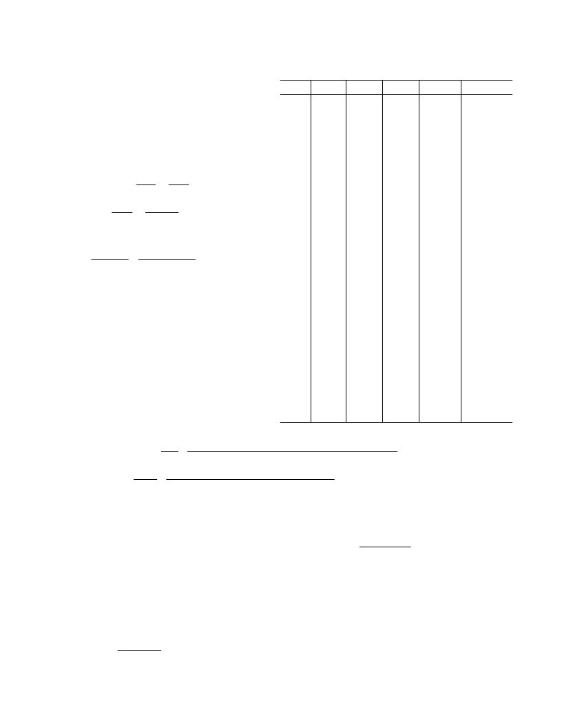
T able I. Output Voltage vs. VID Code
VID3
VID2
VID1
VID0
VID25
V
OUT (NOM)
0
0
0
0
0
0
0
0
0
0
1
1
1
1
1
1
1
1
1
1
1
1
1
1
1
1
0
0
0
0
0
0
1
1
0
0
0
0
0
0
0
0
1
1
1
1
1
1
1
1
0
0
0
0
0
0
0
0
1
1
1
1
1
1
0
0
1
1
1
1
0
0
0
0
1
1
1
1
0
0
0
0
1
1
1
1
0
0
0
0
1
1
1
1
0
0
0
0
1
1
0
0
1
1
0
0
1
1
0
0
1
1
0
0
1
1
0
0
1
1
0
0
1
1
0
0
1
1
0
1
0
1
0
1
0
1
0
1
0
1
0
1
0
1
0
1
0
1
0
1
0
1
0
1
0
1
0
1
0
1
1.050 V
1.075 V
1.100 V
1.125 V
1.150 V
1.175 V
1.200 V
1.225 V
1.250 V
1.275 V
1.300 V
1.325 V
1.350 V
1.375 V
1.400 V
1.425 V
1.450 V
1.475 V
1.500 V
1.525 V
1.550 V
1.575 V
1.600 V
1.625 V
1.650 V
1.675 V
1.700 V
1.725 V
1.750 V
1.775 V
1.800 V
1.825 V
f
t
V
I
R
R
R
–
V
V
I
R
R
R
R
s
V
23
A
6
m
+
m
V
6
V
A
m
m
m
m
MIN
OFF
IN
–
O MAX
(
DS ON HSF
(
SENSE
L
OUT
IN
O(
23
(
DS(
+
3
2 5
.
SENSE
L
DS(
=
×
×
+
+
(
)
×
+
+
(
)
=
×
×
×
+
1
1
3 3
.
5
6
5
3
–
–
–
(
)–1 8
–
–
)
)
)
)
)
μ
)
=
183
kHz
(3)
Inductance Selection
The choice of inductance determines the ripple current in the
inductor. Less inductance leads to more ripple current, which
increases the output ripple voltage and the conduction losses in
the MOSFETs, but allows using smaller-size inductors and, for
a specified peak-to-peak transient deviation, output capacitors
with less total capacitance. Conversely, a higher inductance
means lower ripple current and reduced conduction losses, but
requires larger-size inductors and more output capacitance for
the same peak-to-peak transient deviation. The following equa-
tion shows the relationship between the inductance, oscillator
frequency, peak-to-peak ripple current in an inductor and input
and output voltages:
For 6 A peak-to-peak ripple current, which corresponds to
approximately 25% of the 23 A full-load dc current in an inductor,
Equation 4 yields an inductance of:
×
1 8
3 3
6
L
V
s
A
nH
=
=
990
.
.
μ
A 1
μ
H inductor can be used, which gives a calculated ripple
current of 5.9 A at no load. The inductor should not saturate at
the peak current of 26 A and should be able to handle the sum
of the power dissipation caused by the average current of 23 A
in the winding and the core loss.
L
V
t
I
OUT
OFF
L(
=
×
)
(4)
相關PDF資料 |
PDF描述 |
|---|---|
| ADP3170 | Charger front end protection IC with 30V max Vin and 4.5V LDO output 8-WSON 0 to 125 |
| ADP3171JR | Charger front end protection IC with 30V max Vin and 4.5V LDO output 8-WSON 0 to 125 |
| ADP3171 | Charger front end protection IC with 30V max Vin and 4.5V LDO output 8-WSON 0 to 125 |
| ADP3179 | 4-Bit Programmable Synchronous Buck Controllers |
| ADP3179JRU | PRECISION THERMOSTATS |
相關代理商/技術參數 |
參數描述 |
|---|---|
| ADP3170JRU-REEL7 | 制造商:Analog Devices 功能描述: |
| ADP3170JRUZ-R7 | 制造商:Rochester Electronics LLC 功能描述: 制造商:Analog Devices 功能描述: |
| ADP3170JRUZ-REEL7 | 功能描述:IC CTRLR VRM 8.5 W/REG 20TSSOP RoHS:是 類別:集成電路 (IC) >> PMIC - 穩壓器 - 專用型 系列:- 產品培訓模塊:Lead (SnPb) Finish for COTS Obsolescence Mitigation Program 標準包裝:2,000 系列:- 應用:電源,ICERA E400,E450 輸入電壓:4.1 V ~ 5.5 V 輸出數:10 輸出電壓:可編程 工作溫度:-40°C ~ 85°C 安裝類型:表面貼裝 封裝/外殼:42-WFBGA,WLCSP 供應商設備封裝:42-WLP 包裝:帶卷 (TR) |
| ADP3171 | 制造商:AD 制造商全稱:Analog Devices 功能描述:Synchronous Buck Controller with Dual Linear Regulator Controllers |
| ADP3171JR | 制造商:Rochester Electronics LLC 功能描述:1.2V VTT BUCK CNTRLR W/2 LDOS & PWR GOOD - Bulk |
發布緊急采購,3分鐘左右您將得到回復。