- 您現(xiàn)在的位置:買賣IC網(wǎng) > PDF目錄374022 > ADP3419 (Analog Devices, Inc.) Dual Bootstrapped, High Voltage MOSFET Driver with Output Disable PDF資料下載
參數(shù)資料
| 型號: | ADP3419 |
| 廠商: | Analog Devices, Inc. |
| 英文描述: | Dual Bootstrapped, High Voltage MOSFET Driver with Output Disable |
| 中文描述: | 雙自舉,高電壓MOSFET的輸出驅(qū)動器禁用 |
| 文件頁數(shù): | 6/16頁 |
| 文件大小: | 317K |
| 代理商: | ADP3419 |
ADP3419
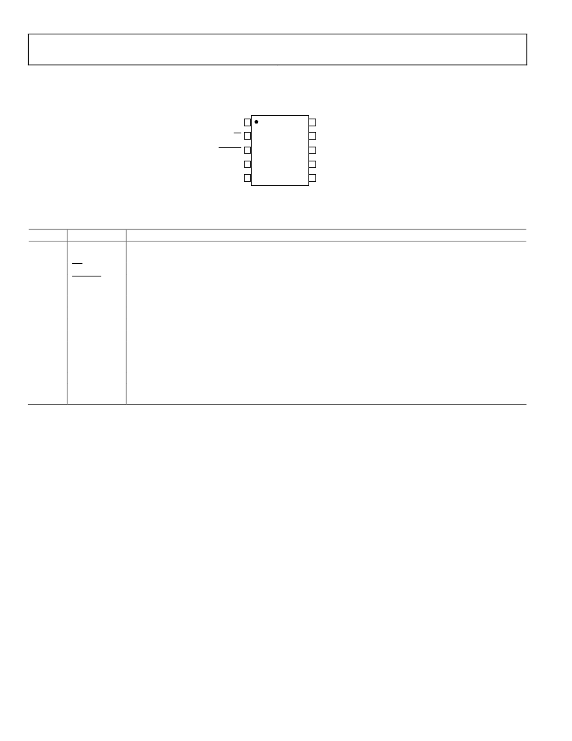
PIN CONFIGURATION AND FUNCTION DESCRIPTIONS
Rev. A | Page 6 of 16
ADP3419
TOP VIEW
(Not to Scale)
IN
SD
DRVLSD
CROWBAR
VCC
BST
DRVH
SW
GND
DRVL
1
2
3
10
9
8
4
5
6
7
0
Figure 5. Pin Configuration
Table 3. Pin Function Descriptions
Pin No.
Mnemonic
1
IN
Function
Logic Level PWM Input. This pin has primary control of the drive outputs. In normal operation, pulling this pin
low turns on the low-side driver; pulling it high turns on the high-side driver.
Shutdown Input. When low, this pin disables normal operation, forcing DRVH and DRVL low.
Synchronous Rectifier Shutdown Input. When low, DRVL is forced low; when high, DRVL is enabled and
controlled by IN and by the adaptive overlap protection control circuitry.
Crowbar Input. When high, DRVL is forced high regardless of the high-side MOSFET switch condition.
Input Supply. This pin should be bypassed to GND with a 4.7 μF or larger ceramic capacitor.
Synchronous Rectifier Drive. Output drive for the lower (synchronous rectifier) MOSFET.
Ground. This pin should be closely connected to the source of the lower MOSFET.
Switch Node Input. This pin is connected to the buck-switching node, close to the upper MOSFET’s source. It is
the floating return for the upper MOSFET drive signal. It is also used to monitor the switched voltage to prevent
turn-on of the lower MOSFET until the voltage is below ~1 V.
Buck Drive. Output drive for the upper (buck) MOSFET.
Upper MOSFET Floating Bootstrap Supply. A capacitor connected between the BST and SW pins holds this
bootstrapped voltage for the high-side MOSFET as it is switched.
2
3
SD
DRVLSD
4
5
6
7
8
CROWBAR
VCC
DRVL
GND
SW
9
10
DRVH
BST
相關(guān)PDF資料 |
PDF描述 |
|---|---|
| ADP3419JRM-REEL | Dual Bootstrapped, High Voltage MOSFET Driver with Output Disable |
| ADP3419JRMZ-REEL1 | Dual Bootstrapped, High Voltage MOSFET Driver with Output Disable |
| ADP3421 | Geyserville-Enabled DC-DC Converter Controller for Mobile CPUs |
| ADP3421JRU | Geyserville-Enabled DC-DC Converter Controller for Mobile CPUs |
| ADP3422 | Secondary Over-Voltage Protection for 2-4 cell in series Li-Ion/Poly (4.35V) 8-TSSOP -40 to 110 |
相關(guān)代理商/技術(shù)參數(shù) |
參數(shù)描述 |
|---|---|
| ADP34190091RMZR | 制造商:ONSEMI 制造商全稱:ON Semiconductor 功能描述:Dual Bootstrapped, High Voltage MOSFET Driver with Output Disable |
| ADP3419JRM-REEL | 功能描述:IC MOSFET DVR DUAL BOOTST 10MSOP RoHS:否 類別:集成電路 (IC) >> PMIC - MOSFET,電橋驅(qū)動器 - 外部開關(guān) 系列:- 標(biāo)準(zhǔn)包裝:95 系列:- 配置:半橋 輸入類型:PWM 延遲時間:25ns 電流 - 峰:1.6A 配置數(shù):1 輸出數(shù):2 高端電壓 - 最大(自引導(dǎo)啟動):118V 電源電壓:9 V ~ 14 V 工作溫度:-40°C ~ 125°C 安裝類型:表面貼裝 封裝/外殼:8-SOIC(0.154",3.90mm 寬) 供應(yīng)商設(shè)備封裝:8-SOIC 包裝:管件 產(chǎn)品目錄頁面:1282 (CN2011-ZH PDF) 其它名稱:*LM5104M*LM5104M/NOPBLM5104M |
| ADP3419JRMZ | 制造商:Analog Device 功能描述: 制造商:Analog Devices 功能描述:MOSFET Driver, Dual, 10 Pin, Plastic, TSSOP |
| ADP3419JRMZ-REEL | 功能描述:功率驅(qū)動器IC DUAL SYNCHRONOUS DRV RoHS:否 制造商:Micrel 產(chǎn)品:MOSFET Gate Drivers 類型:Low Cost High or Low Side MOSFET Driver 上升時間: 下降時間: 電源電壓-最大:30 V 電源電壓-最小:2.75 V 電源電流: 最大功率耗散: 最大工作溫度:+ 85 C 安裝風(fēng)格:SMD/SMT 封裝 / 箱體:SOIC-8 封裝:Tube |
| ADP3419JRMZ-REEL1 | 制造商:AD 制造商全稱:Analog Devices 功能描述:Dual Bootstrapped, High Voltage MOSFET Driver with Output Disable |
發(fā)布緊急采購,3分鐘左右您將得到回復(fù)。