- 您現(xiàn)在的位置:買賣IC網(wǎng) > PDF目錄374022 > ADP3421 (Analog Devices, Inc.) Geyserville-Enabled DC-DC Converter Controller for Mobile CPUs PDF資料下載
參數(shù)資料
| 型號: | ADP3421 |
| 廠商: | Analog Devices, Inc. |
| 元件分類: | DC/DC變換器 |
| 英文描述: | Geyserville-Enabled DC-DC Converter Controller for Mobile CPUs |
| 中文描述: | 蓋瑟維爾啟用的DC - DC轉(zhuǎn)換器控制器的移動處理器 |
| 文件頁數(shù): | 4/12頁 |
| 文件大小: | 146K |
| 代理商: | ADP3421 |
REV. A
ADP3421
–4–
CAUTION
ESD (electrostatic discharge) sensitive device. Electrostatic charges as high as 4000 V readily
accumulate on the human body and test equipment and can discharge without detection.
Although the ADP3421 features proprietary ESD protection circuitry, permanent damage may
occur on devices subjected to high energy electrostatic discharges. Therefore, proper ESD
precautions are recommended to avoid performance degradation or loss of functionality.
WARNING!
ESD SENSITIVE DEVICE
ABSOLUTE MAXIMUM RATINGS
*
Input Supply Voltage (VCC) . . . . . . . . . . . . . . –0.3 V to +7 V
UVLO Input Voltage . . . . . . . . . . . . . . . . . . . . –0.3 V to +7 V
All Other Inputs/Outputs . . . . . . . . . . . . . . . . . . VCC + 0.3 V
Operating Ambient Temperature Range . . . . . . 0
°
C to 100
°
C
Junction Temperature Range . . . . . . . . . . . . . . . 0
°
C to 150
°
C
θ
JA
. . . . . . . . . . . . . . . . . . . . . . . . . . . . . . . . . . . . . . . . 98
°
C/W
Storage Temperature Range . . . . . . . . . . . . –65
°
C to +150
°
C
Lead Temperature (Soldering, 10 sec.) . . . . . . . . . . . . . 300
°
C
*
Stresses above those listed under Absolute Maximum Ratings may cause perma-
nent damage to the device. This is a stress rating only; functional operation of the
device at these or any other conditions above those indicated in the operational
section of this specification is not implied. Exposure to absolute maximum rating
conditions for extended periods may affect device reliability.
ORDERING GUIDE
Temperature
Range
Package
Description
Package
Option
Model
ADP3421JRU 0
°
C to 100
°
C
Thin Shrink Small
Outline (TSSOP)
RU-28
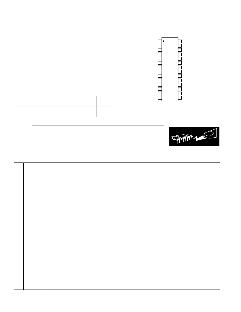
PIN CONFIGURATION
TOP VIEW
(Not to Scale)
28
27
26
25
24
23
22
21
20
19
18
17
16
15
1
2
3
4
5
6
7
8
9
10
11
12
13
14
ADP3421
IOFB
IODRV
CLKFB
CLKDRV
VID0
VID1
VID2
VHYS
CLSET
LTO
LTI
VID3
VID4
LTB
SD
PWRGD
UVLO
SSC
CORE
DACOUT
CS
–
CS+
REG
GND
OUT
VCC
SSL
RAMP
PIN FUNCTION DESCRIPTIONS
Pin
Mnemonic
Function
1
VHYS
Core Comparator Hysteresis Setting. The voltage at this pin is held at a 1.7 V reference level. A resistor to
ground programs at a 1:1 ratio the current that is alternately switched into and out of the RAMP pin.
Current Limit Setting. The voltage at this pin is held at a 1.7 V reference level. A resistor to ground programs
a current that is gained up by 3:1 flowing out of the CS– pin, assuming the current limit comparator is not
triggered.
Level Translator Output. This pin must be tied through a pull-up resistor to the voltage level desired for the
output high level. That voltage cannot be less than 1.5V.
Level Translator Input. This pin should be driven from an open drain/collector signal. The pull-up current is
provided by the pull-up resistor on the LTO pin. However, the pull-up current will be terminated when the
LTI pin reaches 1.5 V.
Level Translator Bypass. For operation of the level translator with high-speed signals, this pin should be by-
passed to ground with a large value capacitor.
VID Input. Most significant bit.
VID Input
VID Input
VID Input
VID Input. Least significant bit.
2.5 V Linear Regulator Driver Output. This pin sinks current from the base of a PNP transistor as needed to
keep the CLKFB node regulated at 2.5 V.
2.5 V Linear Regulator Output Feedback. This pin is connected to the collector of a PNP transistor whose
base is driven by the CLKDRV pin.
1.5 V Linear Regulator Driver Output. This pin sinks current from the base of a PNP transistor as needed to
keep the IOFB node regulated at 1.5 V.
1.5 V Linear Regulator Output Feedback. This pin is connected to the collector of a PNP transistor whose
base is driven by the IODRV pin.
2
CLSET
3
LTO
4
LTI
5
LTB
6
7
8
9
10
11
VID4
VID3
VID2
VID1
VID0
CLKDRV
12
CLKFB
13
IODRV
14
IOFB
相關(guān)PDF資料 |
PDF描述 |
|---|---|
| ADP3421JRU | Geyserville-Enabled DC-DC Converter Controller for Mobile CPUs |
| ADP3422 | Secondary Over-Voltage Protection for 2-4 cell in series Li-Ion/Poly (4.35V) 8-TSSOP -40 to 110 |
| ADP3422JRU | Secondary Over-Voltage Protection for 2-4 cell in series Li-Ion/Poly (4.40V) 8-SM8 -40 to 110 |
| ADP3502 | CDMA Power Management System |
| ADP3502ASU | CDMA Power Management System |
相關(guān)代理商/技術(shù)參數(shù) |
參數(shù)描述 |
|---|---|
| ADP3421JRU | 制造商:AD 制造商全稱:Analog Devices 功能描述:Geyserville-Enabled DC-DC Converter Controller for Mobile CPUs |
| ADP3421JRU-REEL | 制造商:Rochester Electronics LLC 功能描述: 制造商:Analog Devices 功能描述: |
| ADP3421JRU-REEL7 | 制造商:ON Semiconductor 功能描述: |
| ADP3422 | 制造商:AD 制造商全稱:Analog Devices 功能描述:IMVP-II-Compliant Core Power Controller for Mobile CPUs |
| ADP3422JRU | 制造商:AD 制造商全稱:Analog Devices 功能描述:IMVP-II-Compliant Core Power Controller for Mobile CPUs |
發(fā)布緊急采購,3分鐘左右您將得到回復(fù)。