- 您現在的位置:買賣IC網 > PDF目錄374022 > ADP3502ASU (ANALOG DEVICES INC) CDMA Power Management System PDF資料下載
參數資料
| 型號: | ADP3502ASU |
| 廠商: | ANALOG DEVICES INC |
| 元件分類: | 電源管理 |
| 英文描述: | CDMA Power Management System |
| 中文描述: | 2-CHANNEL POWER SUPPLY SUPPORT CKT, PQFP64 |
| 封裝: | 7 X 7 MM, 1 MM HEIGHT, PLASTIC, MS-026ABD, TQFP-64 |
| 文件頁數: | 30/36頁 |
| 文件大小: | 714K |
| 代理商: | ADP3502ASU |
第1頁第2頁第3頁第4頁第5頁第6頁第7頁第8頁第9頁第10頁第11頁第12頁第13頁第14頁第15頁第16頁第17頁第18頁第19頁第20頁第21頁第22頁第23頁第24頁第25頁第26頁第27頁第28頁第29頁當前第30頁第31頁第32頁第33頁第34頁第35頁第36頁
REV. 0
–30–
ADP3502
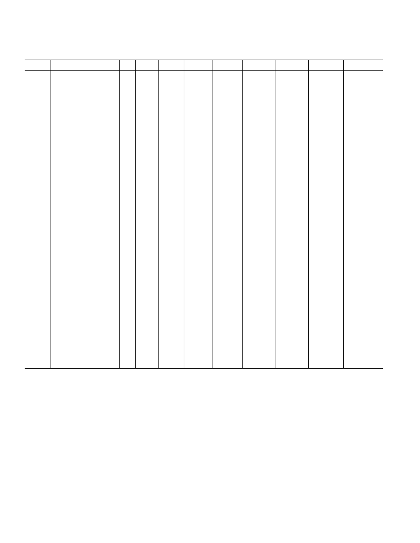
Table V. Registers
ADDR
Description
D7
D6
D5
D4
D3
D2
D1
D0
Comments
00h
01h
02h
03h
04h
05h
06h
07h
08h
09h
0Ah
0Bh
0Ch
0Dh
0Eh
0Fh
10h
11h
12h
13h
14h
15h
16h
17h
18h
19h
1Ah
1Bh
1Ch
Second Counter
Minute Counter
Hour Counter
Week Counter
Day Counter
Month Counter
Year Counter
Alarm A Minute
Alarm A Hour
Alarm A Week
Alarm B Minute
Alarm B Hour
Alarm B Week
Alarm Control
Periodic Interrupt Control
Stay-Alive Timer Control
Charger Control
Charger MVBAT Control
Charger MVBAT
LDO Control 1
Not Available
LDO Control 2
LDO Control 3
LDO2 Gain
Keypad Column/LED
Keypad Row Input
GPIO Control
GPIO MASK
GPIO
S5
M5
S4
M4
H4
S3
M3
H3
S2
M2
H2
W2
D2
MO2
Y2
AM2
AH2
AW2
BM2
BH2
BW2
AOUT
PI2
SA2
S1
M1
H1
W1
D1
MO1
Y1
AM1
AH1
AW1
BM1
BH1
BW1
ALB EN
PI1
SA1
CHI
REF0
MV1
LDO5
S0
M0
H0
W0
D0
MO0
Y0
AM0
AH0
AW0
BM0
BH0
BW0
BOUT
PI0
SA0
CHEN
MVEN
MV0
LDO4
Note 1, 2
Note 1, 2
Note 1, 2
Note 1, 2
Note 1, 2
Note 1, 2
Note 1, 2
Note 2
Note 2
Note 2
Note 2
Note 2
Note 2
Note 2
Note 2
Note 2
Note 3
Note 3
Note 3
Note 3
Note 4
Note 3
Note 3
Note 3
Note 5
Note 5
Note 5
Note 5
Note 5
Note 5
Note 5, 6
Note 5, 6
Note 5, 6
Note 5, 6
Note 5
Note 5
Note 5
Note 5
Note 2, 7
D4
D3
MO3
Y3
AM3
AH3
AW3
BM3
BH3
BW3
ALA EN
PIC
SA3
Y6
Y5
AM5
Y4
AM4
AH4
AW4
BM4
BH4
BW4
AW6
AW5
BM5
BW6
BW5
CLR
SA4
CHV1 CHV0
MV4
MV3
MV2
LDO11
SLEEP9
SLEEP7
LDO10
LDO9
LDO8
LDO7
ALLOFF
G20
KO0
KI0
GPC0
GPMSK0
GPIO
GPO0
GPINT0
GPRST0
INT0
IRST0
MSK0
DI0
PWROFF
PWRON
TEST
G23
KO3
KI3
GPC3
GPMSK3
GPI3
GPO3
GPINT3
GPRST3
INT3
IRST3
MSK3
DI3
G22
KO2
KI2
GPC2
GPMSK2
GPI2
GPO2
GPINT2
GPRST2
INT2
IRST2
MSK2
DI2
G21
KO1
KI1
GPC1
GPMSK1
GPI1
GPO1
GPINT1
GPRST1
INT1
IRST1
MSK1
DI1
BL
KI4
KI5
1Dh
GPIO INT
1Eh
INT
INT6
IRST6 INT5
MSK6 MSK5
INT5
INT4
INT4
MSK4
DI4
1Fh
20h
21h
22h
3Fh
INT MASK
DATA IN
Power OFF
Power ON
TEST Register (Option)
DI5
LDOENB
USENB
NOTES
1. For RTC counter data protection, access should wait for a certain time period (62
μ
s) after the CS signal assertion. (Refer to the RTC Counter Operation section
for the wait time).
2. Registers regarding the RTC counter. They are powered by RTCV.
3. Analog block control registers. They control LDO and so on. They are powered by VBAT.
4. Not available.
5. These are the registers for INT, GPIO, KEYPAD I/F, and so on. They are powered by VBAT.
6. The INT reset operation will be valid at 62
μ
s or later after it’s set.
7. This is a set register for an internal test and should not be accessed at normal operation.
相關PDF資料 |
PDF描述 |
|---|---|
| ADP3510 | Secondary Over-Voltage Protection for 2-4 cell in series Li-Ion/Poly (4.40V) 8-SM8 -40 to 110 |
| ADP3510ARU | Secondary Over-Voltage Protection for 2-4 cell in series Li-Ion/Poly (4.40V) 8-SM8 -40 to 110 |
| ADP3522 | GSM Power Management System |
| ADP3522ACP-1.8 | GSM Power Management System |
| ADP3522ACP-3 | GSM Power Management System |
相關代理商/技術參數 |
參數描述 |
|---|---|
| ADP3502ASU-REEL | 制造商:Analog Devices 功能描述:CDMA Power Management System 64-Pin TQFP T/R |
| ADP3510 | 制造商:AD 制造商全稱:Analog Devices 功能描述:CDMA Power Management System |
| ADP3510ARU | 制造商:AD 制造商全稱:Analog Devices 功能描述:CDMA Power Management System |
| ADP3510ARU-REEL7 | 制造商:Analog Devices 功能描述: |
| ADP3522 | 制造商:AD 制造商全稱:Analog Devices 功能描述:GSM Power Management System |
發布緊急采購,3分鐘左右您將得到回復。