- 您現(xiàn)在的位置:買賣IC網(wǎng) > Datasheet目錄39 > ADP5041ACPZ-1-R7 (Analog Devices Inc)IC REG TRPL BCK/LINEAR 20-LFCSP Datasheet資料下載
參數(shù)資料
| 型號: | ADP5041ACPZ-1-R7 |
| 廠商: | Analog Devices Inc |
| 文件頁數(shù): | 32/40頁 |
| 文件大小: | 3581K |
| 描述: | IC REG TRPL BCK/LINEAR 20-LFCSP |
| 標準包裝: | 1 |
| 拓撲: | 降壓(降壓)同步(1),線性(LDO)(2) |
| 功能: | 任何功能 |
| 輸出數(shù): | 3 |
| 頻率 - 開關: | 3MHz |
| 電壓/電流 - 輸出 1: | 0.8 V ~ 3.8 V,1.2A |
| 電壓/電流 - 輸出 2: | 0.8 V ~ 5.2 V,300mA |
| 電壓/電流 - 輸出 3: | 0.8 V ~ 5.2 V,300mA |
| 帶 LED 驅(qū)動器: | 無 |
| 帶監(jiān)控器: | 是 |
| 帶序列發(fā)生器: | 無 |
| 電源電壓: | 2.3 V ~ 5.5 V |
| 工作溫度: | -40°C ~ 125°C |
| 安裝類型: | 表面貼裝 |
| 封裝/外殼: | 20-WFQFN 裸露焊盤,CSP |
| 供應商設備封裝: | 20-LFCSP-WQ(4x4) |
| 包裝: | 標準包裝 |
| 其它名稱: | ADP5041ACPZ-1-R7DKR |
第1頁第2頁第3頁第4頁第5頁第6頁第7頁第8頁第9頁第10頁第11頁第12頁第13頁第14頁第15頁第16頁第17頁第18頁第19頁第20頁第21頁第22頁第23頁第24頁第25頁第26頁第27頁第28頁第29頁第30頁第31頁當前第32頁第33頁第34頁第35頁第36頁第37頁第38頁第39頁第40頁
ADP5041
Data Sheet
Rev. 0 | Page 32 of 40
Capacitors with lower equivalent series resistance (ESR) are
preferred to guarantee low output voltage ripple, as shown in
the following equation:
IPPLE
RIPPLE
COUT
I
V
SR
d
The effective capacitance needed for stability, which includes
temperature and dc bias effects, is a minimum of 7 礔 and a
maximum of 40 礔.
Table 10. Suggested 10 糉 Capacitors
Vendor
Type Model
Case
Size
Voltage
Rating (V)
Murata
X5R
GRM188R60J106
0603
6.3
Taiyo
Yuden
X5R
JMK107BJ106MA-T
0603
6.3
TDK
X5R
C1608JB0J106K
0603
6.3
Panasonic X5R
ECJ1VB0J106M
0603
6.3
The buck regulator requires 10 礔 output capacitors to guaran-
tee stability and response to rapid load variations and to transition
in and out the PWM/PSM modes. In certain applications where
the buck regulator powers a processor, the operating state is
known because it is controlled by software. In this condition,
the processor can drive the MODE pin according to the operating
state; consequently, it is possible to reduce the output capacitor
from 10 礔 to 4.7 礔 because the regulator does not expect a
large load variation when working in PSM mode (see Figure 109).
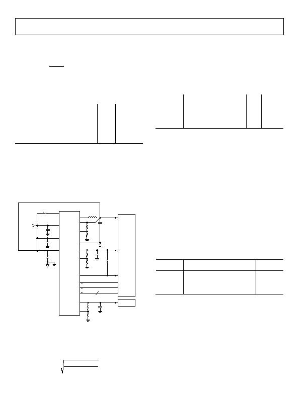
SW
VIN1
VIN2
VIN3
VOUT1
VOUT2
PGND
VOUT3
L1
1礖
R7
100k&
C1
10礔
C2
1礔
C3
1礔
AVIN
R
FLT
30&
V
IN
.3V TO 5.5V
MICRO PMU
ADP5041
PROCESSOR
ANALOG
SUBSYSTEM
VCORE
VDDIO
RESET
GPIO1
MODE
WDI
GPIO2
ENx
GPIO[x:y]
3
R5
FB3
R6
R1
R2
R3
R4
VANALOG
nRSTO
FB1
FB2
C6
2.2礔
C5
4.7礔
C7
2.2礔
Figure 109. Processor System Power Management with PSM/PWM Control
Input Capacitor
A higher value input capacitor helps to reduce the input voltage
ripple and improve transient response. Maximum input
capacitor current is calculated using the following equation:
IN
OUT
IN
OUT
MAX
LOAD
CIN
V
V
V
V
I
)
(
)
(
e
To minimize supply noise, place the input capacitor as close
to the VIN pin of the buck as possible. As with the output
capacitor, a low ESR capacitor is recommended.
The effective capacitance needed for stability, which includes
temperature and dc bias effects, is a minimum of 3 礔 and a
maximum of 10 礔. A list of suggested capacitors is shown in
Table 11.
Table 11. Suggested 4.7 糉 Capacitors
Vendor
Type Model
Case
Size
Voltage
Rating
(V)
Murata
X5R
GRM188R60J475ME19D 0603 6.3
Taiyo Yuden X5R
JMK107BJ475
0603 6.3
Panasonic
X5R
ECJ-0EB0J475M
0402 6.3
LDO EXTERNAL COMPONENT SELECTION
Feedback Resistors
The maximum value of Rb is not to exceed 200 k?(see
Figure 103).
OUTPUT CAPACITOR
The ADP5041 LDOs are designed for operation with small,
space-saving ceramic capacitors, but they function with most
commonly used capacitors as long as care is taken with the ESR
value. The ESR of the output capacitor affects stability of the
LDO control loop. A minimum of 0.70 礔 capacitance with an
ESR of 1 & or less is recommended to ensure stability of the
LDO. Transient response to changes in load current is also
affected by output capacitance. Using a larger value of output
capacitance improves the transient response of the LDO to large
changes in load current.
When operating at output currents higher than 200 mA a
minimum of 2.2 礔 capacitance with an ESR of 1 & or less is
recommended to ensure stability of the LDO.
Table 12. Suggested 2.2 糉 Capacitors
Vendor
Type Model
Case
Size
Voltage
Rating (V)
Murata
X5R
GRM188B31A225K 0402 10.0
TDK
X5R
C1608JB0J225KT
0402 6.3
Panasonic
X5R
ECJ1VB0J225K
0402 6.3
Taiyo Yuden X5R
JMK107BJ225KK-T
0402 6.3
Input Bypass Capacitor
Connecting 1 礔 capacitors from VIN2 and VIN3 to ground
reduces the circuit sensitivity to printed circuit board (PCB)
layout, especially when long input traces or high source
impedance is encountered. If greater than 1 礔 of output
capacitance is required, increase the input capacitor to match it.
相關PDF資料 |
PDF描述 |
|---|---|
| ADP5042ACPZ-2-R7 | IC REG TRPL BCK/LINEAR 20LFCSP |
| ADT6402SRJZ-RL7 | IC TEMP SENS TRIP PT PP SOT-23-6 |
| ADT6501SRJZP085RL7 | IC TEMP SENSOR MICROPWR SOT23-5 |
| ADT7302ARTZ-500RL7 | IC SENSOR TEMP 13BIT DGT SOT23-6 |
| ADT7310TRZ | IC TEMP SENSOR 16BIT SPI 8SOIC |
相關代理商/技術(shù)參數(shù) |
參數(shù)描述 |
|---|---|
| ADP5041CP-1-EVALZ | 功能描述:ADP5041 - DC/DC, Step Down with LDO 3, Non-Isolated Outputs Evaluation Board 制造商:analog devices inc. 系列:- 零件狀態(tài):有效 主要用途:DC/DC,LDO 步降 輸出和類型:3,非隔離 功率 - 輸出:- 電壓 - 輸出:- 電流 - 輸出:1.2A,300mA,300mA 電壓 - 輸入:2.3 V ~ 5.5 V 穩(wěn)壓器拓撲:降壓 頻率 - 開關:3MHz 板類型:完全填充 所含物品:板 使用的 IC/零件:ADP5041 標準包裝:1 |
| ADP5042 | 制造商:AD 制造商全稱:Analog Devices 功能描述:Micro PMU with 0.8 A Buck, Two 300 mA LDOs Supervisory, Watchdog and Manual Reset |
| ADP5042ACPZ-1 | 制造商:Analog Devices 功能描述:PMU 2 LDO DUAL BUCK 20LFCSP 制造商:Analog Devices 功能描述:PMU, 2 LDO, DUAL BUCK, 20LFCSP |
| ADP5042ACPZ-1-R7 | 功能描述:IC REG TRPL BCK/LINEAR 20LFCSP RoHS:是 類別:集成電路 (IC) >> PMIC - 穩(wěn)壓器 - 線性 + 切換式 系列:- 標準包裝:2,500 系列:- 拓撲:降壓(降壓)同步(3),線性(LDO)(2) 功能:任何功能 輸出數(shù):5 頻率 - 開關:300kHz 電壓/電流 - 輸出 1:控制器 電壓/電流 - 輸出 2:控制器 電壓/電流 - 輸出 3:控制器 帶 LED 驅(qū)動器:無 帶監(jiān)控器:無 帶序列發(fā)生器:是 電源電壓:5.6 V ~ 24 V 工作溫度:-40°C ~ 85°C 安裝類型:* 封裝/外殼:* 供應商設備封裝:* 包裝:* |
| ADP5042ACPZ-2 | 制造商:Analog Devices 功能描述:PMU 2 LDO DUAL BUCK 20LFCSP 制造商:Analog Devices 功能描述:PMU, 2 LDO, DUAL BUCK, 20LFCSP |
發(fā)布緊急采購,3分鐘左右您將得到回復。