- 您現在的位置:買賣IC網 > PDF目錄374034 > ADSP-2171BS-133 (ANALOG DEVICES INC) DSP Microcomputer PDF資料下載
參數資料
| 型號: | ADSP-2171BS-133 |
| 廠商: | ANALOG DEVICES INC |
| 元件分類: | 數字信號處理 |
| 英文描述: | DSP Microcomputer |
| 中文描述: | 24-BIT, 16.67 MHz, OTHER DSP, PQFP128 |
| 封裝: | PLASTIC, QFP-128 |
| 文件頁數: | 10/52頁 |
| 文件大小: | 664K |
| 代理商: | ADSP-2171BS-133 |
第1頁第2頁第3頁第4頁第5頁第6頁第7頁第8頁第9頁當前第10頁第11頁第12頁第13頁第14頁第15頁第16頁第17頁第18頁第19頁第20頁第21頁第22頁第23頁第24頁第25頁第26頁第27頁第28頁第29頁第30頁第31頁第32頁第33頁第34頁第35頁第36頁第37頁第38頁第39頁第40頁第41頁第42頁第43頁第44頁第45頁第46頁第47頁第48頁第49頁第50頁第51頁第52頁
REV. A
–10–
ADSP-2171/ADSP-2172/ADSP-2173
Bus Request & Bus Grant
T he ADSP-217x can relinquish control of the data and address
buses to an external device. When the external device requires
access to memory, it asserts the bus request (
BR
) signal. If the
ADSP-217x is not performing an external memory access, then
it responds to the active
BR
input in the following processor
cycle by:
three-stating the data and address buses and the
PMS
,
DMS
,
BMS
,
RD
,
WR
output drivers,
asserting the bus grant (
BG
) signal, and
halting program execution.
If the Go Mode is enabled, the ADSP-217x will not halt pro-
gram execution until it encounters an instruction that requires
an external memory access.
If the ADSP-217x is performing an external memory access
when the external device asserts the
BR
signal, then it will not
three-state the memory interfaces or assert the
BG
signal until
the processor cycle after the access completes, which can be up
to eight cycles later depending on the number of wait states.
T he instruction does not need to be completed when the bus is
granted. If a single instruction requires two external memory ac-
cesses, the bus will be granted between the two accesses.
When the
BR
signal is released, the processor releases the
BG
signal, reenables the output drivers and continues program ex-
ecution from the point where it stopped.
T he bus request feature operates at all times, including when
the processor is booting and when
RESET
is active.
T he new Bus Grant Hang logic and associated
BGH
pin allow
the ADSP-217x to operate in a multiprocessor environment
with a minimal number of “wasted” processor cycles. T he bus
grant hang pin is asserted when the ADSP-217x desires a cycle,
but cannot execute it because the bus is granted to some other
processor. With the
BGH
signal, the other processor(s) in the
system can be alerted that the ADSP-217x is hung and release
the bus by deasserting bus request. Once the bus is released the
ADSP-217x executes the external access and deasserts
BGH
.
T his is a signal to the other processors that external memory is
now available.
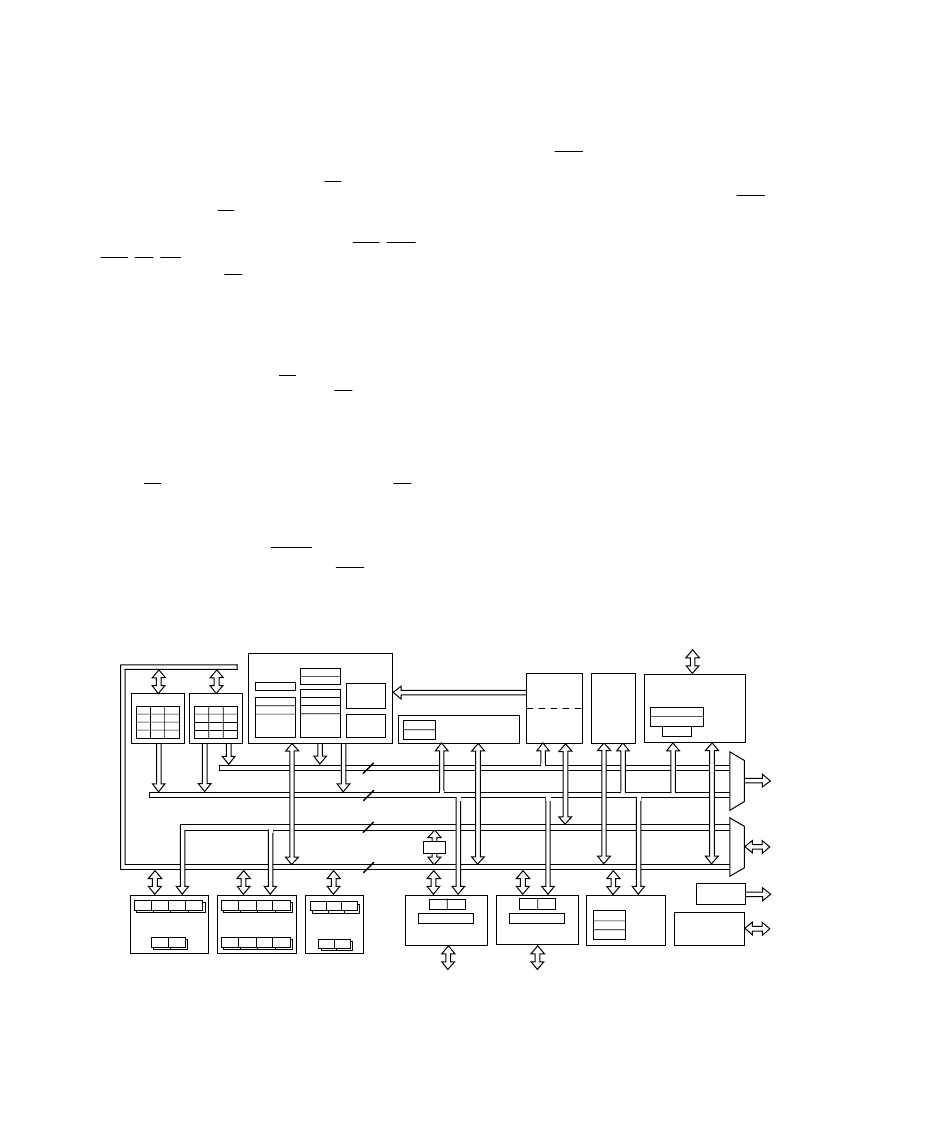
ADSP-217X RE GIST E RS
Figure 7 summarizes all the registers in the ADSP-217x. Some
registers store values. For example, AX 0 stores an ALU oper-
and; I4 stores a DAG2 pointer. Other registers consist of control
bits and fields, or status flags. For example, AST AT contains
status flags from arithmetic operations, and fields in DWAIT
control the numbers of wait states for different zones of data
memory.
A secondary set of registers in all computational units allows a
single-cycle context switch.
T he bit and field definitions for control and status registers are
given in the rest of this section, except for IMASK , ICNT L and
IFC, which are defined earlier in this data sheet. T he system
control register, DWAIT register, timer registers, HIP control
registers, HIP data registers, and SPORT control registers are
all mapped into data memory; that is, registers are accessed by
reading and writing data memory locations rather than register
names. T he particular data memory address is shown with each
memory-mapped register.
Register bit values shown on the following pages are the default
bit values after reset. If no values are shown, the bits are indeter-
minate at reset. Reserved bits are shown in gray; these bits
should always be written with zeros.
MAC
MR0 MR1
MF
MR2
MX0 MX1 MY0 MY1
DMA BUS
PMA BUS
DMD BUS
PMD BUS
14
POWERDOWN
CONTROL
LOGIC
PROGRAM
ROM
8K X 24
PROGRAM
SRAM
2K X 24
DAG 2
M4
M5
M6
M7
I7
L4
L5
L6
L7
I4
I5
I6
DAG 1
M0
M1
M2
M3
I3
L0
L1
L2
L3
I0
I1
I2
PROGRAM SEQUENCER
ICNTL
IFC
4 X 14
CNTR
OWRCNTR
STACK
12 X 25
IMASK
MSTAT
ASTAT
SSTAT
SPC
4 X 18
DM WAIT CONTROL
SYSTEM CONTROL
0x3FFF
0x3FFE
HOST
INTERFACE
PORT
DATA
STATUS
HMASK
0x3FE0-0x3FE5
0x3FE6-0x3FE7
0x3FE8
ALU
AF
AR
AX0
AY1
AY0
AX1
SHIFTER
SR0 SR1
SI
SE
SB
SPORT 1
CONTROL REGISTERS
0x3FF2-0x3FEF
RX1
TX1
SPORT 0
CONTROL REGISTERS
0x3FFA-0x3FF3
RX0
TX0
PX
TIMER
TPERIOD
TCOUNT
TSCALE
0x3FFD
0x3FFC
0x3FFB
FLAGS
14
16
24
DATA
SRAM
2K X 16
Figure 7. ADSP-217x Registers Control Register
相關PDF資料 |
PDF描述 |
|---|---|
| ADSP-2173BST-80 | DSP Microcomputer |
| ADSP-2171KS-104 | CAP 4.7PF 50V +/-0.5PF NPO(C0G) SMD-0603 TR-7-PA |
| ADSP-2171KS-133 | DSP Microcomputer |
| ADSP-2171KST-104 | DSP Microcomputer |
| ADSP-2171KST-133 | DSP Microcomputer |
相關代理商/技術參數 |
參數描述 |
|---|---|
| ADSP-2171BST-104 | 制造商:Rochester Electronics LLC 功能描述:- Bulk |
| ADSP-2171BST-133 | 制造商:Analog Devices 功能描述:DSP Fixed-Point 16-Bit 33.33MHz 33MIPS 128-Pin TQFP 制造商:Rochester Electronics LLC 功能描述:16BIT FXD PT PROC 33 MIPS - Bulk 制造商:Analog Devices 功能描述:IC MICROCOMPUTER 16-BIT |
| ADSP-2171BSTZ-133 | 功能描述:IC DSP CONTROLLER 16BIT 128TQFP RoHS:是 類別:集成電路 (IC) >> 嵌入式 - DSP(數字式信號處理器) 系列:ADSP-21xx 標準包裝:2 系列:StarCore 類型:SC140 內核 接口:DSI,以太網,RS-232 時鐘速率:400MHz 非易失內存:外部 芯片上RAM:1.436MB 電壓 - 輸入/輸出:3.30V 電壓 - 核心:1.20V 工作溫度:-40°C ~ 105°C 安裝類型:表面貼裝 封裝/外殼:431-BFBGA,FCBGA 供應商設備封裝:431-FCPBGA(20x20) 包裝:托盤 |
| ADSP-2171BSZ-133 | 功能描述:IC DSP CONTROLLER 16BIT 128PQFP RoHS:是 類別:集成電路 (IC) >> 嵌入式 - DSP(數字式信號處理器) 系列:ADSP-21xx 標準包裝:40 系列:TMS320DM64x, DaVinci™ 類型:定點 接口:I²C,McASP,McBSP 時鐘速率:400MHz 非易失內存:外部 芯片上RAM:160kB 電壓 - 輸入/輸出:3.30V 電壓 - 核心:1.20V 工作溫度:0°C ~ 90°C 安裝類型:表面貼裝 封裝/外殼:548-BBGA,FCBGA 供應商設備封裝:548-FCBGA(27x27) 包裝:托盤 配用:TMDSDMK642-0E-ND - DEVELPER KIT W/NTSC CAMERA296-23038-ND - DSP STARTER KIT FOR TMS320C6416296-23059-ND - FLASHBURN PORTING KIT296-23058-ND - EVAL MODULE FOR DM642TMDSDMK642-ND - DEVELOPER KIT W/NTSC CAMERA |
| ADSP-2171KS-104 | 制造商:Analog Devices 功能描述:DSP Fixed-Point 16-Bit 26MHz 26MIPS 128-Pin PQFP 制造商:Rochester Electronics LLC 功能描述:- Bulk |
發布緊急采購,3分鐘左右您將得到回復。