- 您現(xiàn)在的位置:買(mǎi)賣(mài)IC網(wǎng) > PDF目錄374034 > ADSP-2171BS-133 (ANALOG DEVICES INC) DSP Microcomputer PDF資料下載
參數(shù)資料
| 型號(hào): | ADSP-2171BS-133 |
| 廠商: | ANALOG DEVICES INC |
| 元件分類(lèi): | 數(shù)字信號(hào)處理 |
| 英文描述: | DSP Microcomputer |
| 中文描述: | 24-BIT, 16.67 MHz, OTHER DSP, PQFP128 |
| 封裝: | PLASTIC, QFP-128 |
| 文件頁(yè)數(shù): | 8/52頁(yè) |
| 文件大小: | 664K |
| 代理商: | ADSP-2171BS-133 |
第1頁(yè)第2頁(yè)第3頁(yè)第4頁(yè)第5頁(yè)第6頁(yè)第7頁(yè)當(dāng)前第8頁(yè)第9頁(yè)第10頁(yè)第11頁(yè)第12頁(yè)第13頁(yè)第14頁(yè)第15頁(yè)第16頁(yè)第17頁(yè)第18頁(yè)第19頁(yè)第20頁(yè)第21頁(yè)第22頁(yè)第23頁(yè)第24頁(yè)第25頁(yè)第26頁(yè)第27頁(yè)第28頁(yè)第29頁(yè)第30頁(yè)第31頁(yè)第32頁(yè)第33頁(yè)第34頁(yè)第35頁(yè)第36頁(yè)第37頁(yè)第38頁(yè)第39頁(yè)第40頁(yè)第41頁(yè)第42頁(yè)第43頁(yè)第44頁(yè)第45頁(yè)第46頁(yè)第47頁(yè)第48頁(yè)第49頁(yè)第50頁(yè)第51頁(yè)第52頁(yè)
REV. A
–8–
ADSP-2171/ADSP-2172/ADSP-2173
Program Memory Interface
T he on-chip program memory address bus (PMA) and the on-
chip program memory data bus (PMD) are multiplexed with
on-chip DMA and DMD buses, creating a single external data
bus and a single external address bus. T he 14-bit address bus
directly addresses up to 16K words. 10K words of memory for
ADSP-217x with optional 8K ROM and 2K words of memory
for the non-ROM version are on-chip. T he data bus is bidirec-
tional and 24 bits wide to external program memory. Program
memory may contain code and data.
T he program memory data lines are bidirectional. T he program
memory select (
PMS
) signal indicates access to the program
memory and can be used as a chip select signal. T he write (
WR
)
signal indicates a write operation and is used as a write strobe.
T he read (
RD
) signal indicates a read operation and is used as a
read strobe or output enable signal.
T he ADSP-217x writes data from its 16-bit registers to the 24-
bit program memory using the PX register to provide the lower
eight bits. When it reads data (not instructions) from 24-bit pro-
gram memory to a 16-bit data register, the lower eight bits are
placed in the PX register.
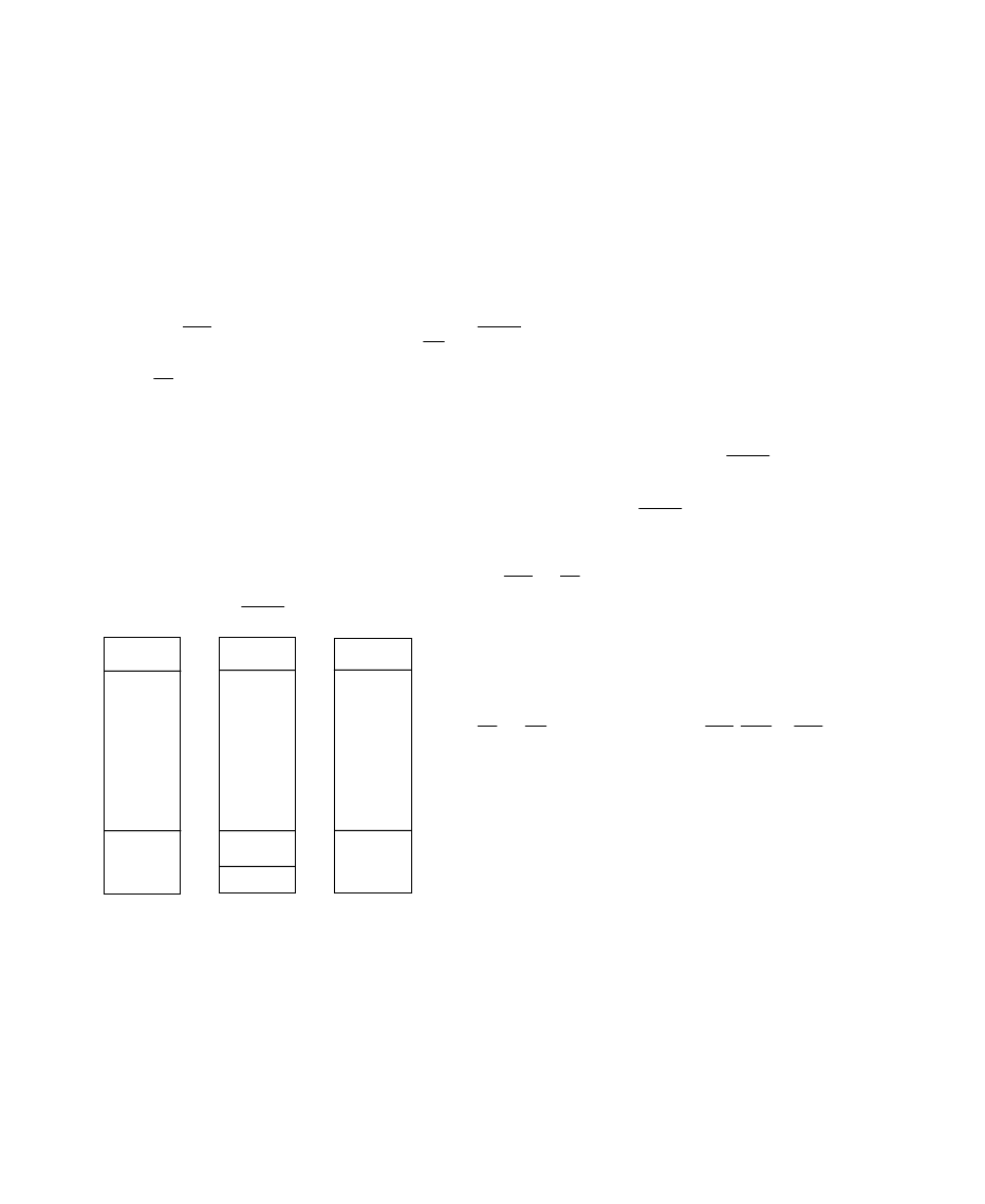
Program Memory Maps
ADSP-217x
Program memory can be mapped in two ways, depending on the
state of the MMAP pin. Figure 5 shows the different configura-
tions. When MMAP = 0, internal RAM occupies 2K words be-
ginning at address 0x0000. In this configuration, the boot
loading sequence (described in “Boot Memory Interface”) is au-
tomatically initiated when
RESET
is released.
37FF
3800
3FFF
0000
MMAP = 1
BMODE = 0
2K
EXTERNAL
27FF
2800
8K
INTERNAL ROM
(ROMENABLE = 1)
OR
4K
EXTERNAL
2K
INTERNAL RAM
07FF
0800
8K
EXTERNAL
(ROMENABLE = 0)
2K
INTERNAL RAM
NOT BOOTED
6K
EXTERNAL
3FFF
0000
27FF
2800
07FF
0800
MMAP = 1
BMODE = 1
8K
INTERNAL ROM
(ROMENABLE
DEFAULTS
TO 1
DURING RESET)
MMAP = 0
BMODE = 0 or 1
2K
INTERNAL RAM
BOOTED
6K
EXTERNAL
3FFF
0000
27FF
2800
07FF
0800
OR
8K
EXTERNAL
(ROMENABLE = 0)
8K
INTERNAL ROM
(ROMENABLE = 1)
Figure 5. ADSP-217x Memory Maps
When MMAP = 1, words of external program memory begin at
address 0x0000 and internal RAM is located in the upper 2K
words, beginning at address 0x3800. In this configuration, pro-
gram memory is not loaded although it can be written to and
read from under program control.
T he optional ROM always resides at locations PM[0x0800]
through PM[0x27FF] regardless of the state of the MMAP pin.
T he ROM is enabled by setting the ROMENABLE bit in the
Data Memory Wait State control register, DM[0x3FFE]. When
the ROMENABLE bit is set to 1, addressing program memory
in this range will access the on-chip ROM. When set to zero,
addressing program memory in this range will access external
program memory. T he ROMENABLE bit is set to 0 on chip re-
set unless MMAP
and
BMODE = 1.
T he program memory interface can generate 0 to 7 wait states
for external memory devices; default is to 7 wait states after
RESET
.
Boot Memory Interface
T he ADSP-217x can load on-chip memory from external boot
memory space. T he boot memory space consists of 64K by 8-bit
space, divided into eight separate 8K by 8-bit pages. T hree bits
in the system control register select which page is loaded by the
boot memory interface. Another bit in the system control regis-
ter allows the user to force a boot loading sequence under soft-
ware control. Boot loading from page 0 after
RESET
is initiated
automatically if MMAP = 0.
T he boot memory interface can generate 0 to 7 wait states; it
defaults to 7 wait states after
RESET
. T his allows the ADSP-
217x to boot from a single low cost EPROM such as a 27C256.
Program memory is booted one byte at a time and converted to
24-bit program memory words.
T he
BMS
and
RD
signals are used to select and to strobe the
boot memory interface. Only 8-bit data is read over the data
bus, on pins D8–D15. T o accommodate addressing up to eight
pages of boot memory, the two MSBs of the data bus are used
in the boot memory interface as the two MSBs of the boot space
address.
T he ADSP-2100 Family Assembler and Linker support the cre-
ation of programs and data structures requiring multiple boot
pages during execution.
RD
and
WR
must always be qualified by
PMS
,
DMS
, or
BMS
to ensure the correct program, data, or boot memory accessing.
HIP Booting
T he ADSP-217x can also boot programs through its Host Inter-
face Port. If BMODE = 1 and MMAP = 0, the ADSP-217x
boots from the HIP. If BMODE = 0, the ADSP-217x boots
through the data bus (in the same way as the ADSP-2101), as
described above in “Boot Memory Interface.” For additional in-
formation about HIP booting, refer to the
ADSP-2100 Family
User’s Manual
, Chapter 7, “Host Interface Port.”
T he ADSP-2100 Family Development Software includes a util-
ity program called the HIP Splitter. T his utility allows the cre-
ation of programs that can be booted via the ADSP-217x’s HIP,
in a similar fashion as EPROM-bootable programs generated by
the PROM Splitter utility.
相關(guān)PDF資料 |
PDF描述 |
|---|---|
| ADSP-2173BST-80 | DSP Microcomputer |
| ADSP-2171KS-104 | CAP 4.7PF 50V +/-0.5PF NPO(C0G) SMD-0603 TR-7-PA |
| ADSP-2171KS-133 | DSP Microcomputer |
| ADSP-2171KST-104 | DSP Microcomputer |
| ADSP-2171KST-133 | DSP Microcomputer |
相關(guān)代理商/技術(shù)參數(shù) |
參數(shù)描述 |
|---|---|
| ADSP-2171BST-104 | 制造商:Rochester Electronics LLC 功能描述:- Bulk |
| ADSP-2171BST-133 | 制造商:Analog Devices 功能描述:DSP Fixed-Point 16-Bit 33.33MHz 33MIPS 128-Pin TQFP 制造商:Rochester Electronics LLC 功能描述:16BIT FXD PT PROC 33 MIPS - Bulk 制造商:Analog Devices 功能描述:IC MICROCOMPUTER 16-BIT |
| ADSP-2171BSTZ-133 | 功能描述:IC DSP CONTROLLER 16BIT 128TQFP RoHS:是 類(lèi)別:集成電路 (IC) >> 嵌入式 - DSP(數(shù)字式信號(hào)處理器) 系列:ADSP-21xx 標(biāo)準(zhǔn)包裝:2 系列:StarCore 類(lèi)型:SC140 內(nèi)核 接口:DSI,以太網(wǎng),RS-232 時(shí)鐘速率:400MHz 非易失內(nèi)存:外部 芯片上RAM:1.436MB 電壓 - 輸入/輸出:3.30V 電壓 - 核心:1.20V 工作溫度:-40°C ~ 105°C 安裝類(lèi)型:表面貼裝 封裝/外殼:431-BFBGA,F(xiàn)CBGA 供應(yīng)商設(shè)備封裝:431-FCPBGA(20x20) 包裝:托盤(pán) |
| ADSP-2171BSZ-133 | 功能描述:IC DSP CONTROLLER 16BIT 128PQFP RoHS:是 類(lèi)別:集成電路 (IC) >> 嵌入式 - DSP(數(shù)字式信號(hào)處理器) 系列:ADSP-21xx 標(biāo)準(zhǔn)包裝:40 系列:TMS320DM64x, DaVinci™ 類(lèi)型:定點(diǎn) 接口:I²C,McASP,McBSP 時(shí)鐘速率:400MHz 非易失內(nèi)存:外部 芯片上RAM:160kB 電壓 - 輸入/輸出:3.30V 電壓 - 核心:1.20V 工作溫度:0°C ~ 90°C 安裝類(lèi)型:表面貼裝 封裝/外殼:548-BBGA,F(xiàn)CBGA 供應(yīng)商設(shè)備封裝:548-FCBGA(27x27) 包裝:托盤(pán) 配用:TMDSDMK642-0E-ND - DEVELPER KIT W/NTSC CAMERA296-23038-ND - DSP STARTER KIT FOR TMS320C6416296-23059-ND - FLASHBURN PORTING KIT296-23058-ND - EVAL MODULE FOR DM642TMDSDMK642-ND - DEVELOPER KIT W/NTSC CAMERA |
| ADSP-2171KS-104 | 制造商:Analog Devices 功能描述:DSP Fixed-Point 16-Bit 26MHz 26MIPS 128-Pin PQFP 制造商:Rochester Electronics LLC 功能描述:- Bulk |
發(fā)布緊急采購(gòu),3分鐘左右您將得到回復(fù)。