- 您現(xiàn)在的位置:買賣IC網(wǎng) > PDF目錄374035 > ADSP-2184L (Analog Devices, Inc.) LM2941/LM2941C 1A Low Dropout Adjustable Regulator; Package: TO-220; No of Pins: 5; Qty per Container: 45; Container: Rail PDF資料下載
參數(shù)資料
| 型號: | ADSP-2184L |
| 廠商: | Analog Devices, Inc. |
| 英文描述: | LM2941/LM2941C 1A Low Dropout Adjustable Regulator; Package: TO-220; No of Pins: 5; Qty per Container: 45; Container: Rail |
| 中文描述: | DSP的微機 |
| 文件頁數(shù): | 11/31頁 |
| 文件大小: | 216K |
| 代理商: | ADSP-2184L |
第1頁第2頁第3頁第4頁第5頁第6頁第7頁第8頁第9頁第10頁當前第11頁第12頁第13頁第14頁第15頁第16頁第17頁第18頁第19頁第20頁第21頁第22頁第23頁第24頁第25頁第26頁第27頁第28頁第29頁第30頁第31頁
ADSP-2184L
–11–
REV. 0
Flag I/O Pins
The ADSP-2184L has eight general purpose programmable input/
output flag pins. They are controlled by two memory mapped
registers. The PFTYPE register determines the direction,
1 = output and 0 = input. The PFDATA register is used to read
and write the values on the pins. Data being read from a pin
configured as an input is synchronized to the ADSP-2184L’s
clock. Bits that are programmed as outputs will read the value
being output. The PF pins default to input during reset.
In addition to the programmable flags, the ADSP-2184L has
five fixed-mode flags, FLAG_IN, FLAG_OUT, FL0, FL1 and
FL2. FL0-FL2 are dedicated output flags. FLAG_IN and
FLAG_OUT are available as an alternate configuration of
SPORT1.
Note: Pins PF0, PF1 and PF2 are also used for device configu-
ration during reset.
INSTRUCTION SET DESCRIPTION
The ADSP-2184L assembly language instruction set has an
algebraic syntax that was designed for ease of coding and
readability. The assembly language, which takes full advantage
of the processor’s unique architecture, offers the following benefits:
The algebraic syntax eliminates the need to remember cryptic
assembler mnemonics. For example, a typical arithmetic add
instruction, such as AR = AX0 + AY0, resembles a simple
equation.
Every instruction assembles into a single, 24-bit word that
can execute in a single instruction cycle.
The syntax is a superset ADSP-2100 Family assembly lan-
guage and is completely source and object code compatible
with other family members. Programs may need to be relo-
cated to utilize on-chip memory and conform to the ADSP-
2184L’s interrupt vector and reset vector map.
Sixteen condition codes are available. For conditional jump,
call, return or arithmetic instructions, the condition can be
checked and the operation executed in the same instruction
cycle.
Multifunction instructions allow parallel execution of an
arithmetic instruction with up to two fetches or one write to
processor memory space during a single instruction cycle.
DESIGNING AN EZ-ICE-COMPATIBLE SYSTEM
The ADSP-2184L has on-chip emulation support and an
ICE-Port, a special set of pins that interface to the EZ-ICE. These
features allow in-circuit emulation without replacing the target
system processor by using only a 14-pin connection from the
target system to the EZ-ICE. Target systems must have a 14-pin
connector to accept the EZ-ICE’s in-circuit probe, a 14-pin plug.
Issuing the chip reset command during emulation causes the
DSP to perform a full chip reset, including a reset of its memory
mode. Therefore, it is vital that the mode pins are set correctly
PRIOR to issuing a chip reset command from the emulator user
interface.
If using a passive method of maintaining mode information (as
discussed in Setting Memory Modes), it does not matter that
the mode information is latched by an emulator reset. However,
if using the
RESET
pin as a method of setting the value of the
mode pins, the effects of an emulator reset must be taken into
consideration.
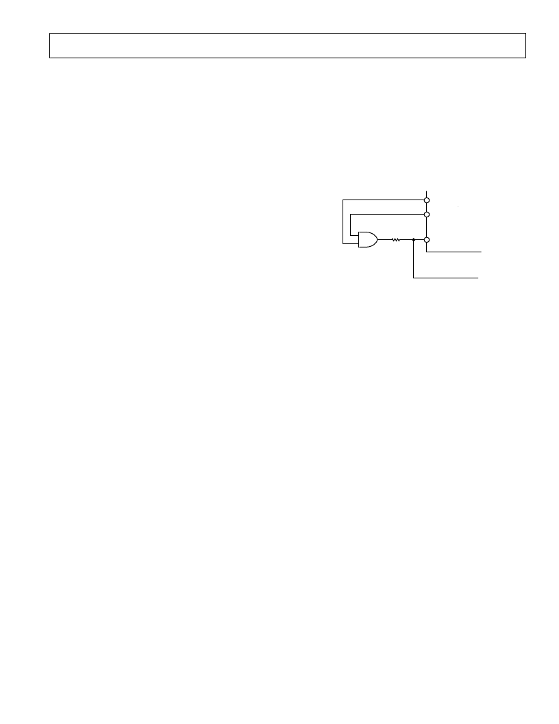
One method of ensuring that the values located on the mode
pins are the desired values is to construct a circuit like the one
shown in Figure 7. This circuit forces the value located on the
Mode A pin to logic low, regardless if it latched via the
RESET
or
ERESET
pin.
1k
V
ERESET
RESET
MODE A/PF0
ADSP-2184L
PROGRAMMABLE I/O
Figure 7. Boot Mode Circuit
See the
ADSP-2100 Family EZ-Tools
data sheet for complete
information on ICE products.
The ICE-Port interface consists of the following ADSP-2184L
pins:
EBR
EBG
ERESET
EMS
EINT
ECLK
ELIN
ELOUT
EE
These ADSP-2184L pins are usually connected only to the
EZ-ICE
connector in the target system. These pins have no
function except during emulation, and do not require pull-up
or pull-down resistors. The traces for these signals between
the ADSP-2184L and the connector must be kept as short as
possible, no longer than three inches.
The following pins are also used by the EZ-ICE:
BR
BG
RESET
GND
The EZ-ICE
uses the EE (emulator enable) signal to take con-
trol of the ADSP-2184L in the target system. This causes the
processor to use its
ERESET
,
EBR
and
EBG
pins instead of
the
RESET
,
BR
and
BG
pins. The
BG
output is three-stated.
These signals do not need to be jumper-isolated in your system.
The EZ-ICE connects to your target system via a ribbon cable
and a 14-pin female plug. The female plug is plugged onto the
14-pin connector (a pin strip header) on the target board.
相關(guān)PDF資料 |
PDF描述 |
|---|---|
| ADSP-2184NKST-320 | DSP Microcomputer |
| ADSP-2186NKCA-320 | DSP Microcomputer |
| ADSP-2184N | DSP Microcomputer |
| ADSP-2187N | DSP Microcomputer |
| ADSP-2188 | Cap-Free, NMOS, 150mA Low Dropout Regulator with Reverse Current Protection |
相關(guān)代理商/技術(shù)參數(shù) |
參數(shù)描述 |
|---|---|
| ADSP-2184LBST-160 | 制造商:Analog Devices 功能描述:DSP Fixed-Point 16-Bit 40MHz 40MIPS 100-Pin LQFP 制造商:Analog Devices 功能描述:IC MICROCOMPUTER 16-BIT |
| ADSP-2184LBSTZ-160 | 功能描述:IC DSP CONTROLLER 16BIT 100LQFP RoHS:是 類別:集成電路 (IC) >> 嵌入式 - DSP(數(shù)字式信號處理器) 系列:ADSP-21xx 標準包裝:2 系列:StarCore 類型:SC140 內(nèi)核 接口:DSI,以太網(wǎng),RS-232 時鐘速率:400MHz 非易失內(nèi)存:外部 芯片上RAM:1.436MB 電壓 - 輸入/輸出:3.30V 電壓 - 核心:1.20V 工作溫度:-40°C ~ 105°C 安裝類型:表面貼裝 封裝/外殼:431-BFBGA,F(xiàn)CBGA 供應(yīng)商設(shè)備封裝:431-FCPBGA(20x20) 包裝:托盤 |
| ADSP-2184LBSTZ-1602 | 制造商:AD 制造商全稱:Analog Devices 功能描述:DSP Microcomputer |
| ADSP-2184N | 制造商:AD 制造商全稱:Analog Devices 功能描述:DSP Microcomputer |
| ADSP-2184NBCA-320 | 制造商:Analog Devices 功能描述:DSP Fixed-Point 16-Bit 80MHz 80MIPS 144-Pin CSP-BGA 制造商:Rochester Electronics LLC 功能描述:4K PM/4K DM RAM,16-BIT,80 MIPS, 1.8V - Bulk |
發(fā)布緊急采購,3分鐘左右您將得到回復(fù)。