- 您現在的位置:買賣IC網 > PDF目錄374037 > ADSP-BF531SBBZ400 (ANALOG DEVICES INC) Blackfin Embedded Processor PDF資料下載
參數資料
| 型號: | ADSP-BF531SBBZ400 |
| 廠商: | ANALOG DEVICES INC |
| 元件分類: | 數字信號處理 |
| 英文描述: | Blackfin Embedded Processor |
| 中文描述: | 16-BIT, 40 MHz, OTHER DSP, PBGA169 |
| 封裝: | ROHS COMPLIANT, PLASTIC, MO-034AAG-2, BGA-169 |
| 文件頁數: | 1/56頁 |
| 文件大小: | 671K |
| 代理商: | ADSP-BF531SBBZ400 |
當前第1頁第2頁第3頁第4頁第5頁第6頁第7頁第8頁第9頁第10頁第11頁第12頁第13頁第14頁第15頁第16頁第17頁第18頁第19頁第20頁第21頁第22頁第23頁第24頁第25頁第26頁第27頁第28頁第29頁第30頁第31頁第32頁第33頁第34頁第35頁第36頁第37頁第38頁第39頁第40頁第41頁第42頁第43頁第44頁第45頁第46頁第47頁第48頁第49頁第50頁第51頁第52頁第53頁第54頁第55頁第56頁
a
Blackfin and the Blackfin logo are registered trademarks of Analog Devices, Inc.
Blackfin
Embedded Processor
ADSP-BF531/ADSP-BF532/ADSP-BF533
Rev. 0
Information furnished by Analog Devices is believed to be accurate and reliable.
However, no responsibility is assumed by Analog Devices for its use, nor for any
infringements of patents or other rights of third parties that may result from its use.
Specifications subject to change without notice. No license is granted by implication
or otherwise under any patent or patent rights of Analog Devices. Trademarks and
registered trademarks are the property of their respective owners.
One Technology Way, P.O. Box 9106, Norwood, MA 02062-9106 U.S.A.
Tel: 781.329.4700
Fax: 781.326.8703
www.analog.comFEATURES
Up to 600MHz high performance Blackfin processor
Two 16-bit MACs, two 40-bit ALUs, four 8-bit video ALUs,
40-bit Shifter
RISC-like register and instruction model for ease of pro-
gramming and compiler-friendly support
Advanced debug, trace, and performance monitoring
0.8 V to 1.2 V core V
DD
with on-chip voltage regulation
3.3V and 2.5 V tolerant I/O
160-ball mini-BGA, 169-ball lead free PBGA, and 176-lead
LQFP packages
MEMORY
Up to 148K bytes of on-chip memory:
16K bytes of instruction SRAM/Cache
64K bytes of instruction SRAM
32K bytes of data SRAM/Cache
32K bytes of data SRAM
4K bytes of scratchpad SRAM
Two dual-channel memory DMA controllers
Memory Management Unit providing memory protection
External Memory Controller with glueless support for
SDRAM, SRAM, FLASH, and ROM
Flexible memory booting options from SPI and external
memory
PERIPHERALS
Parallel Peripheral Interface (PPI)/GPIO, supporting
ITU-R 656 video data formats
Two dual-channel, full duplex synchronous serial ports, sup-
porting eight stereo I
2
S channels
12-channel DMA controller
SPI compatible port
Three Timer/Counters with PWM support
UART with support for IrDA
Event Handler
Real-Time Clock
Watchdog Timer
Debug/JTAG interface
On-chip PLL capable of 1x to 63x frequency multiplication
Core Timer
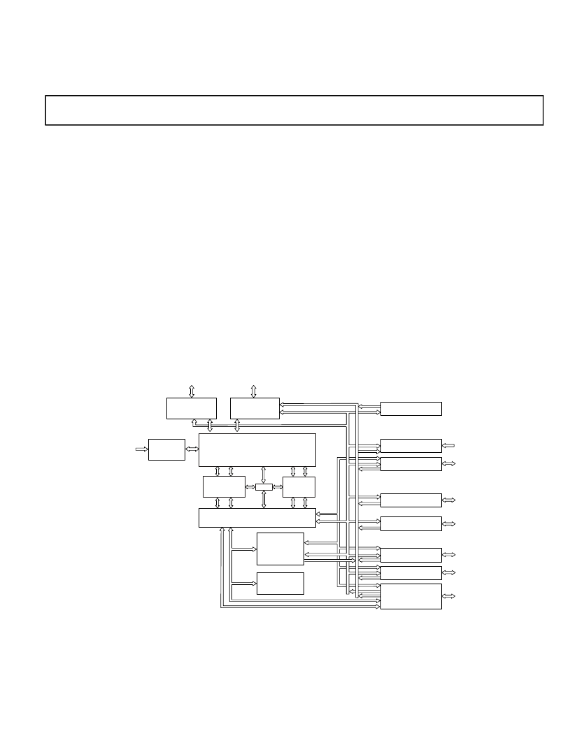
Figure 1. Functional Block Diagram
VOLTAGE
REGULATOR
DMA
CONTROLLER
EVENT
CONTROLLER/
CORE TIMER
REAL-TIME CLOCK
UART PORT
IRDA
TIMER0, TIMER1,
TIMER2
PPI / GPIO
SERIAL PORTS (2)
SPI PORT
EXTERNAL PORT
FLASH, SDRAM
CONTROL
BOOT ROM
JTAG TEST AND
EMULATION
WATCHDOG TIMER
L1
INSTRUCTION
MEMORY
L1
DATA
MEMORY
MMU
CORE / SYSTEM BUS INTERFACE
B
相關PDF資料 |
PDF描述 |
|---|---|
| ADSP-BF531SBST400 | Circular Connector Series:97 |
| ADSP-BF532 | Blackfin Embedded Processor |
| ADSP-BF532SBBC400 | Blackfin Embedded Processor |
| ADSP-BF532SBBZ400 | Blackfin Embedded Processor |
| ADSP-BF532SBST400 | 28-2 (14 Contacts) Pin Insert; For Use With:Amphenol MIL-C-5015 97 Series Circular Connectors; No. of Contacts:14; Gender:Male; Operating Voltage:1250V |
相關代理商/技術參數 |
參數描述 |
|---|---|
| ADSP-BF531SBST-300 | 制造商:Analog Devices 功能描述: |
| ADSP-BF531SBST-300X | 制造商:Analog Devices 功能描述: |
| ADSP-BF531SBST400 | 制造商:Analog Devices 功能描述:DSP Fixed-Point 16-Bit 400MHz 400MIPS 176-Pin LQFP 制造商:Rochester Electronics LLC 功能描述:DUAL MAC16-BIT400MHZ,52KB SRAM - Bulk 制造商:Analog Devices 功能描述:IC MICROCOMPUTER 16-BIT |
| ADSP-BF531SBST-C81 | 制造商:Analog Devices 功能描述: |
| ADSP-BF531SBST-ENG | 制造商:Analog Devices 功能描述: |
發布緊急采購,3分鐘左右您將得到回復。