- 您現在的位置:買賣IC網 > PDF目錄374037 > ADSP-BF532 (Analog Devices, Inc.) Blackfin Embedded Processor PDF資料下載
參數資料
| 型號: | ADSP-BF532 |
| 廠商: | Analog Devices, Inc. |
| 元件分類: | 數字信號處理 |
| 英文描述: | Blackfin Embedded Processor |
| 中文描述: | Blackfin嵌入式處理器 |
| 文件頁數: | 12/56頁 |
| 文件大小: | 671K |
| 代理商: | ADSP-BF532 |
第1頁第2頁第3頁第4頁第5頁第6頁第7頁第8頁第9頁第10頁第11頁當前第12頁第13頁第14頁第15頁第16頁第17頁第18頁第19頁第20頁第21頁第22頁第23頁第24頁第25頁第26頁第27頁第28頁第29頁第30頁第31頁第32頁第33頁第34頁第35頁第36頁第37頁第38頁第39頁第40頁第41頁第42頁第43頁第44頁第45頁第46頁第47頁第48頁第49頁第50頁第51頁第52頁第53頁第54頁第55頁第56頁
Rev. 0
|
Page 12 of 56
|
March 2004
ADSP-BF531/ADSP-BF532/ADSP-BF533
as the RTC, may still be running but will not be able to access
internal resources or external memory. This powered-down
mode can only be exited by assertion of the reset interrupt
(RESET) or by an asynchronous interrupt generated by the
RTC. When in Deep Sleep mode, an RTC asynchronous inter-
rupt causes the processor to transition to the Active mode.
Assertion of RESET while in Deep Sleep mode causes the pro-
cessor to transition to the Full-On mode.
Power Savings
As shown in
Table 5
, the ADSP-BF531/2/3 processor supports
three different power domains. The use of multiple power
domains maximizes flexibility, while maintaining compliance
with industry standards and conventions. By isolating the inter-
nal logic of the ADSP-BF531/2/3 processor into its own power
domain, separate from the RTC and other I/O, the processor
can take advantage of Dynamic Power Management, without
affecting the RTC or other I/O devices. There are no sequencing
requirements for the various power domains.
The power dissipated by a processor is largely a function of the
clock frequency of the processor and the square of the operating
voltage. For example, reducing the clock frequency by 25%
results in a 25% reduction in dynamic power dissipation, while
reducing the voltage by 25% reduces dynamic power dissipation
by more than 40%. Further, these power savings are additive, in
that if the clock frequency and supply voltage are both reduced,
the power savings can be dramatic.
The Dynamic Power Management feature of the ADSP-
BF531/2/3 processor allows both the processor’s input voltage
(V
DDINT
) and clock frequency (f
CCLK
) to be dynamically
controlled.
The savings in power dissipation can be modeled using the
Power Savings Factor and % Power Savings calculations.
The Power Savings Factor is calculated as:
where the variables in the equations are:
f
CCLKNOM
is the nominal core clock frequency
f
CCLKRED
is the reduced core clock frequency
V
DDINTNOM
is the nominal internal supply voltage
V
DDINTRED
is the reduced internal supply voltage
T
NOM
is the duration running at f
CCLKNOM
T
RED
is the duration running at f
CCLKRED
The percent power savings is calculated as:
VOLTAGE REGULATION
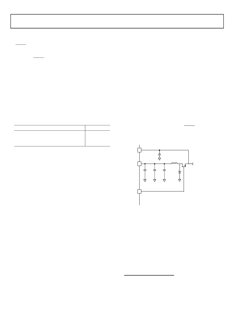
The Blackfin processor provides an on-chip voltage regulator
that can generate processor core voltage levels 0.85V(-5% /
+10%) to 1.2V(-5% / +10%) from an external 2.25 V to 3.6 V
supply.
Figure 7
shows the typical external components
required to complete the power management system.
*
The regu-
lator controls the internal logic voltage levels and is
programmable with the Voltage Regulator Control Register
(VR_CTL) in increments of 50 mV. To reduce standby power
consumption, the internal voltage regulator can be programmed
to remove power to the processor core while keeping I/O power
(V
DDEXT
) supplied. While in hibernation, V
DDEXT
can still be
applied, eliminating the need for external buffers. The voltage
regulator can be activated from this power-down state either
through an RTC wakeup or by asserting RESET, which will then
initiate a boot sequence. The regulator can also be disabled and
bypassed at the user’s discretion.
CLOCK SIGNALS
The ADSP-BF531/2/3 processor can be clocked by an external
crystal, a sine wave input, or a buffered, shaped clock derived
from an external clock oscillator.
If an external clock is used, it should be a TTL compatible signal
and must not be halted, changed, or operated below the speci-
fied frequency during normal operation. This signal is
connected to the processor’s CLKIN pin. When an external
clock is used, the XTAL pin must be left unconnected.
Table 5. Power Domains
Power Domain
All internal logic, except RTC
RTC internal logic and crystal I/O
All other I/O
VDD Range
V
DDINT
V
DDRTC
V
DDEXT
Power Savings Factor
f
CCLKNOM
---------------------
V
DDINTNOM
--------------------------
2
×
T
NOM
------------
×
=
*
See EE-228: Switching Regulator Design Considerations for ADSP-BF533
Blackfin Processors.
Figure 7. Voltage Regulator Circuit
% Power Savings
1
Power Savings Factor
–
(
)
100%
×
=
V
DDEXT
V
DDINT
VR
OUT
1-0
EXTERNAL COMPONENTS
2.25V TO 3.6V
INPUT VOLTAGE
RANGE
NDS8434
ZHCS1000
100 μF
1 μF
10 μH
0.1 μF
NOTE: VR
OUT
1-0SHOULD BE TIED TOGETHER EXTERNALLY
AND DESIGNER SHOULD MINIMIZETRACE LENGTH TO NDS8434.
100 μF
相關PDF資料 |
PDF描述 |
|---|---|
| ADSP-BF532SBBC400 | Blackfin Embedded Processor |
| ADSP-BF532SBBZ400 | Blackfin Embedded Processor |
| ADSP-BF532SBST400 | 28-2 (14 Contacts) Pin Insert; For Use With:Amphenol MIL-C-5015 97 Series Circular Connectors; No. of Contacts:14; Gender:Male; Operating Voltage:1250V |
| ADSP-BF533 | Blackfin Embedded Processor |
| ADSP-BF533SBBC500 | Metal Connector Backshell |
相關代理商/技術參數 |
參數描述 |
|---|---|
| ADSP-BF532SBB400 | 制造商:Analog Devices 功能描述:DSP Fixed-Point 16-Bit 400MHz 400MIPS 169-Pin BGA |
| ADSPBF532SBBC400 | 制造商:Analog Devices 功能描述: |
| ADSP-BF532SBBC400 | 功能描述:IC DSP CTLR 16B 400MHZ 160CSPBGA RoHS:否 類別:集成電路 (IC) >> 嵌入式 - DSP(數字式信號處理器) 系列:Blackfin® 標準包裝:2 系列:StarCore 類型:SC140 內核 接口:DSI,以太網,RS-232 時鐘速率:400MHz 非易失內存:外部 芯片上RAM:1.436MB 電壓 - 輸入/輸出:3.30V 電壓 - 核心:1.20V 工作溫度:-40°C ~ 105°C 安裝類型:表面貼裝 封裝/外殼:431-BFBGA,FCBGA 供應商設備封裝:431-FCPBGA(20x20) 包裝:托盤 |
| ADSP-BF532SBBC400X | 制造商:Analog Devices 功能描述: |
| adsp-bf532sbb-c80 | 制造商:Analog Devices 功能描述: |
發布緊急采購,3分鐘左右您將得到回復。