- 您現(xiàn)在的位置:買(mǎi)賣(mài)IC網(wǎng) > PDF目錄374037 > ADSP-BF533SBBZ500 (ANALOG DEVICES INC) Blackfin Embedded Processor PDF資料下載
參數(shù)資料
| 型號(hào): | ADSP-BF533SBBZ500 |
| 廠商: | ANALOG DEVICES INC |
| 元件分類(lèi): | 數(shù)字信號(hào)處理 |
| 英文描述: | Blackfin Embedded Processor |
| 中文描述: | 16-BIT, 40 MHz, OTHER DSP, PBGA169 |
| 封裝: | ROHS COMPLIANT, PLASTIC, MO-034AAG-2, BGA-169 |
| 文件頁(yè)數(shù): | 42/56頁(yè) |
| 文件大小: | 671K |
| 代理商: | ADSP-BF533SBBZ500 |
第1頁(yè)第2頁(yè)第3頁(yè)第4頁(yè)第5頁(yè)第6頁(yè)第7頁(yè)第8頁(yè)第9頁(yè)第10頁(yè)第11頁(yè)第12頁(yè)第13頁(yè)第14頁(yè)第15頁(yè)第16頁(yè)第17頁(yè)第18頁(yè)第19頁(yè)第20頁(yè)第21頁(yè)第22頁(yè)第23頁(yè)第24頁(yè)第25頁(yè)第26頁(yè)第27頁(yè)第28頁(yè)第29頁(yè)第30頁(yè)第31頁(yè)第32頁(yè)第33頁(yè)第34頁(yè)第35頁(yè)第36頁(yè)第37頁(yè)第38頁(yè)第39頁(yè)第40頁(yè)第41頁(yè)當(dāng)前第42頁(yè)第43頁(yè)第44頁(yè)第45頁(yè)第46頁(yè)第47頁(yè)第48頁(yè)第49頁(yè)第50頁(yè)第51頁(yè)第52頁(yè)第53頁(yè)第54頁(yè)第55頁(yè)第56頁(yè)
Rev. 0
|
Page 42 of 56
|
March 2004
ADSP-BF531/ADSP-BF532/ADSP-BF533
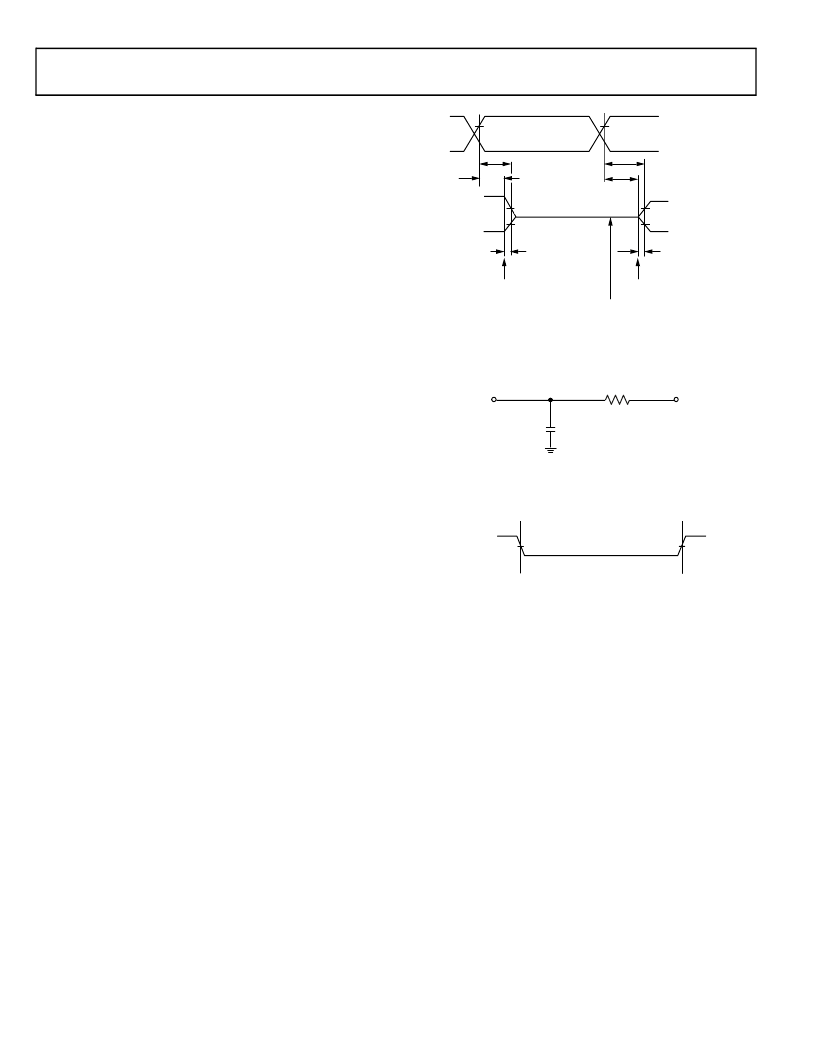
TEST CONDITIONS
All timing parameters appearing in this data sheet were mea-
sured under the conditions described in this section.
Output Enable Time
Output pins are considered to be enabled when they have made
a transition from a high impedance state to the point when they
start driving. The output enable time t
ENA
is the interval from
the point when a reference signal reaches a high or low voltage
level to the point when the output starts driving as shown in the
Output Enable/Disable diagram (
Figure 33
). The time
t
ENA_MEASURED
is the interval from when the reference signal
switches to when the output voltage reaches 2.0 V (output high)
or 1.0 V (output low). Time t
TRIP
is the interval from when the
output starts driving to when the output reaches the 1.0 V or
2.0 V trip voltage. Time t
ENA
is calculated as shown in the
equation:
If multiple pins (such as the data bus) are enabled, the measure-
ment value is that of the first pin to start driving.
Output Disable Time
Output pins are considered to be disabled when they stop driv-
ing, go into a high impedance state, and start to decay from their
output high or low voltage. The time for the voltage on the bus
to decay by
V is dependent on the capacitive load, C
L
and the
load current, I
L
. This decay time can be approximated by the
equation:
The output disable time t
DIS
is the difference between
t
DIS_MEASURED
and t
DECAY
as shown in
Figure 33
. The time
t
DIS_MEASURED
is the interval from when the reference signal
switches to when the output voltage decays
V from the mea-
sured output high or output low voltage. The time t
DECAY
is
calculated with test loads C
L
and I
L
, and with
V equal to 0.5 V.
Example System Hold Time Calculation
To determine the data output hold time in a particular system,
first calculate t
DECAY
using the equation given above. Choose
V to be the difference between the ADSP-BF531/2/3 proces-
sor’s output voltage and the input threshold for the device
requiring the hold time. A typical
V will be 0.4 V. C
L
is the
total bus capacitance (per data line), and I
L
is the total leakage or
three-state current (per data line). The hold time will be t
DECAY
plus the minimum disable time (for example, t
DSDAT
for an
SDRAM write cycle).
Capacitive Loading
Output delays and holds are based on standard capacitive loads:
30 pF on all pins (see
Figure 34
).
Figure 36
through
Figure 43 on
Page 44
show how output rise time varies with capacitance. The
delay and hold specifications given should be derated by a factor
derived from these figures. The graphs in these figures may not
be linear outside the ranges shown.
t
ENA
t
ENA_MEASURED
t
TRIP
–
=
t
DECAY
C
L
V
(
)
I
L
=
Figure 33. Output Enable/Disable
Figure 34. Equivalent Device Loading for AC Measurements
(Includes All Fixtures)
Figure 35. Voltage Reference Levels for AC
Measurements (Except Output Enable/Disable)
REFERENCE
SIGNAL
t
DIS
OUTPUT STARTS DRIVING
V
OH
(MEASURED)
V
V
OL
(MEASURED) +
V
t
DIS_MEASURED
V
OH
(MEASURED)
V
OL
(MEASURED)
2.0V
1.0V
V
OH
(MEASURED)
V
OL
(MEASURED)
t
TRIP
HIGH IMPEDANCE STATE.
TEST CONDITIONS CAUSE THIS
VOLTAGE TO BE APPROXIMATELY 1.5V.
OUTPUT STOPS DRIVING
t
ENA
t
DECAY
t
ENA-MEASURED
1.5V
30pF
TO
OUTPUT
PIN
50 OHMS
INPUT
OR
OUTPUT
1.5V
1.5V
相關(guān)PDF資料 |
PDF描述 |
|---|---|
| ADSP-BF533SKBC600 | Blackfin Embedded Processor |
| ADSP-BF561SKBCZ600 | Blackfin Embedded Symmetric Multi-Processor |
| ADSP-BF561SKBCZ500 | Blackfin Embedded Symmetric Multi-Processor |
| ADSP-BF561 | Synchronous 4-Bit Up/Down Binary Counters With Dual Clock and Clear 16-PDIP 0 to 70 |
| ADSP-BF561SBB500 | Blackfin Embedded Symmetric Multi-Processor |
相關(guān)代理商/技術(shù)參數(shù) |
參數(shù)描述 |
|---|---|
| ADSP-BF533SBBZ500X | 制造商:Analog Devices 功能描述: |
| ADSP-BF533SBST400 | 制造商:Analog Devices 功能描述:DSP Fixed-Point 16-Bit 400MHz 400MIPS 176-Pin LQFP |
| ADSP-BF533SBSTZ400 | 功能描述:IC DSP CTLR 16BIT 400MHZ 176LQFP RoHS:是 類(lèi)別:集成電路 (IC) >> 嵌入式 - DSP(數(shù)字式信號(hào)處理器) 系列:Blackfin® 標(biāo)準(zhǔn)包裝:40 系列:TMS320DM64x, DaVinci™ 類(lèi)型:定點(diǎn) 接口:I²C,McASP,McBSP 時(shí)鐘速率:400MHz 非易失內(nèi)存:外部 芯片上RAM:160kB 電壓 - 輸入/輸出:3.30V 電壓 - 核心:1.20V 工作溫度:0°C ~ 90°C 安裝類(lèi)型:表面貼裝 封裝/外殼:548-BBGA,F(xiàn)CBGA 供應(yīng)商設(shè)備封裝:548-FCBGA(27x27) 包裝:托盤(pán) 配用:TMDSDMK642-0E-ND - DEVELPER KIT W/NTSC CAMERA296-23038-ND - DSP STARTER KIT FOR TMS320C6416296-23059-ND - FLASHBURN PORTING KIT296-23058-ND - EVAL MODULE FOR DM642TMDSDMK642-ND - DEVELOPER KIT W/NTSC CAMERA |
| ADSP-BF533SKBC300X | 制造商:Analog Devices 功能描述: |
| ADSP-BF533SKBC600 | 制造商:Analog Devices 功能描述:DSP Fixed-Point 16-Bit 600MHz 600MIPS 160-Pin CSP-BGA |
發(fā)布緊急采購(gòu),3分鐘左右您將得到回復(fù)。