- 您現在的位置:買賣IC網 > PDF目錄374037 > ADSP21020 (Analog Devices, Inc.) 32/40-Bit IEEE Floating-Point DSP Microprocessor PDF資料下載
參數資料
| 型號: | ADSP21020 |
| 廠商: | Analog Devices, Inc. |
| 元件分類: | 數字信號處理 |
| 英文描述: | 32/40-Bit IEEE Floating-Point DSP Microprocessor |
| 中文描述: | 32/40 IEEE浮點DSP微處理器 |
| 文件頁數: | 24/32頁 |
| 文件大小: | 425K |
| 代理商: | ADSP21020 |
第1頁第2頁第3頁第4頁第5頁第6頁第7頁第8頁第9頁第10頁第11頁第12頁第13頁第14頁第15頁第16頁第17頁第18頁第19頁第20頁第21頁第22頁第23頁當前第24頁第25頁第26頁第27頁第28頁第29頁第30頁第31頁第32頁
ADSP-21020
REV. C
–24–
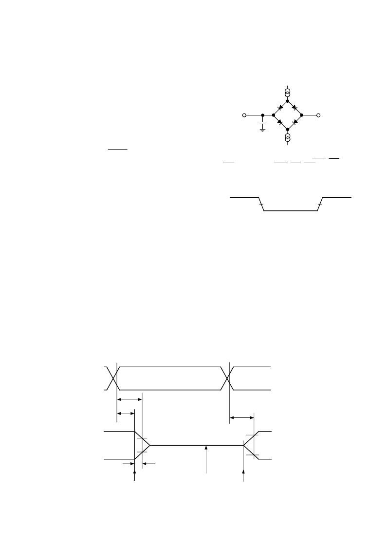
TEST CONDITIONS
Output Disable Time
Output pins are considered to be disabled when they stop
driving, go into a high-impedance state, and start to decay from
their output high or low voltage. The time for the voltage on the
bus to decay by
V is dependent on the capacitive load, C
L
, and
the load current, I
L
. It can be approximated by the following
equation:
t
DECAY
=
C
L
V
I
L
The output disable time (t
DIS
) is the difference between
t
MEASURED
and t
DECAY
as shown in Figure 13. The time
t
MEASURED
) is the interval from when the reference signal
switches to when the output voltage decays
V from the
measured output high or output low voltage. t
DECAY
is
calculated with
V equal to 0.5 V, and test loads C
L
and I
L
.
Output Enable Time
Output pins are considered to be enabled when they have made
a transition from a high-impedance state to when they start
driving. The output enable time (t
ENA
) is the interval from when
a reference signal reaches a high or low voltage level to when the
output has reached a specified high or low trip point, as shown
in the Output Enable/Disable diagram. If multiple pins (such as
the data bus) are enabled, the measurement value is that of the
first pin to start driving.
Example System Hold Time Calculation
To determine the data output hold time in a particular system,
first calculate t
DECAY
using the above equation. Choose
V to be
the difference between the ADSP-21020’s output voltage and
the input threshold for the device requiring the hold time. A
typical
V will be 0.4 V. C
L
is the total bus capacitance (per
data line), and I
L
is the total leakage or three-state current (per
data line). The hold time will be t
DECAY
plus the minimum
disable time (i.e. t
HDWD
for the write cycle).
TO
OUTPUT
PIN
50pF
*
+1.5V
*AC TIMING SPECIFICATIONS ARE CALCULATED FOR 100pF
DERATING ON THE FOLLOWING PINS: PMA23–0, PMS1–0
,
PMRD,
PMWR, PMPAGE, DMA31–0, DMS3–0, DMRD, DMWR, DMPAGE
I
OH
I
OL
Figure 14. Equivalent Device Loading For AC
Measurements (Includes All Fixtures)
INPUT OR
OUTPUT
1.5V
1.5V
Figure 15. Voltage Reference Levels For AC
Measurements (Except Output Enable/Disable)
t
ENA
2.0V
1.0V
–
V
+
V
t
DIS
REFERENCE
SIGNAL
OUTPUT
t
DECAY
V
OH (MEASURED)
V
OL (MEASURED)
t
MEASURED
OUTPUT STOPS DRIVING
OUTPUT STARTS DRIVING
HIGH-IMPEDANCE STATE. TEST CONDITIONS
CAUSE THIS VOLTAGE LEVEL TO BE
APPROXIMATELY 1.5 V.
V
OH (MEASURED)
V
OL (MEASURED)
V
OH (MEASURED)
V
OL (MEASURED)
Figure 13. Output Enable/Disable
相關PDF資料 |
PDF描述 |
|---|---|
| ADSP-21020BG-100 | 32/40-Bit IEEE Floating-Point DSP Microprocessor |
| ADSP2184 | 16 A SPDT MINIATURE POWER RELAY |
| ADSP2185 | DSP Microcomputer |
| ADSP2186 | DSP Microcomputer |
| ADT14 | Circular Connector; No. of Contacts:61; Series:LJT07R; Body Material:Aluminum; Connecting Termination:Crimp; Connector Shell Size:25; Circular Contact Gender:Socket; Circular Shell Style:Jam Nut Receptacle; Insert Arrangement:25-61 |
相關代理商/技術參數 |
參數描述 |
|---|---|
| ADSP-21020 | 制造商:未知廠家 制造商全稱:未知廠家 功能描述: |
| ADSP-21020BG-100 | 制造商:AD 制造商全稱:Analog Devices 功能描述:32/40-Bit IEEE Floating-Point DSP Microprocessor |
| ADSP-21020BG-120 | 制造商:AD 制造商全稱:Analog Devices 功能描述:32/40-Bit IEEE Floating-Point DSP Microprocessor |
| ADSP-21020BG-80 | 制造商:AD 制造商全稱:Analog Devices 功能描述:32/40-Bit IEEE Floating-Point DSP Microprocessor |
| ADSP-21020KG-100 | 制造商:AD 制造商全稱:Analog Devices 功能描述:32/40-Bit IEEE Floating-Point DSP Microprocessor |
發布緊急采購,3分鐘左右您將得到回復。