- 您現在的位置:買賣IC網 > PDF目錄374038 > ADUC7024BST62 (ANALOG DEVICES INC) Precision Analog Microcontroller 12-bit Analog I/O, ARM7TDMI MCU PDF資料下載
參數資料
| 型號: | ADUC7024BST62 |
| 廠商: | ANALOG DEVICES INC |
| 元件分類: | 微控制器/微處理器 |
| 英文描述: | Precision Analog Microcontroller 12-bit Analog I/O, ARM7TDMI MCU |
| 中文描述: | 32-BIT, FLASH, 45.5 MHz, MICROCONTROLLER, PQFP64 |
| 封裝: | PLASTIC, LQFP-64 |
| 文件頁數: | 29/80頁 |
| 文件大小: | 840K |
| 代理商: | ADUC7024BST62 |
第1頁第2頁第3頁第4頁第5頁第6頁第7頁第8頁第9頁第10頁第11頁第12頁第13頁第14頁第15頁第16頁第17頁第18頁第19頁第20頁第21頁第22頁第23頁第24頁第25頁第26頁第27頁第28頁當前第29頁第30頁第31頁第32頁第33頁第34頁第35頁第36頁第37頁第38頁第39頁第40頁第41頁第42頁第43頁第44頁第45頁第46頁第47頁第48頁第49頁第50頁第51頁第52頁第53頁第54頁第55頁第56頁第57頁第58頁第59頁第60頁第61頁第62頁第63頁第64頁第65頁第66頁第67頁第68頁第69頁第70頁第71頁第72頁第73頁第74頁第75頁第76頁第77頁第78頁第79頁第80頁
Preliminary Technical Data
ADuC702x Series
CONVERTER OPERATION
Rev. PrB | Page 29 of 80
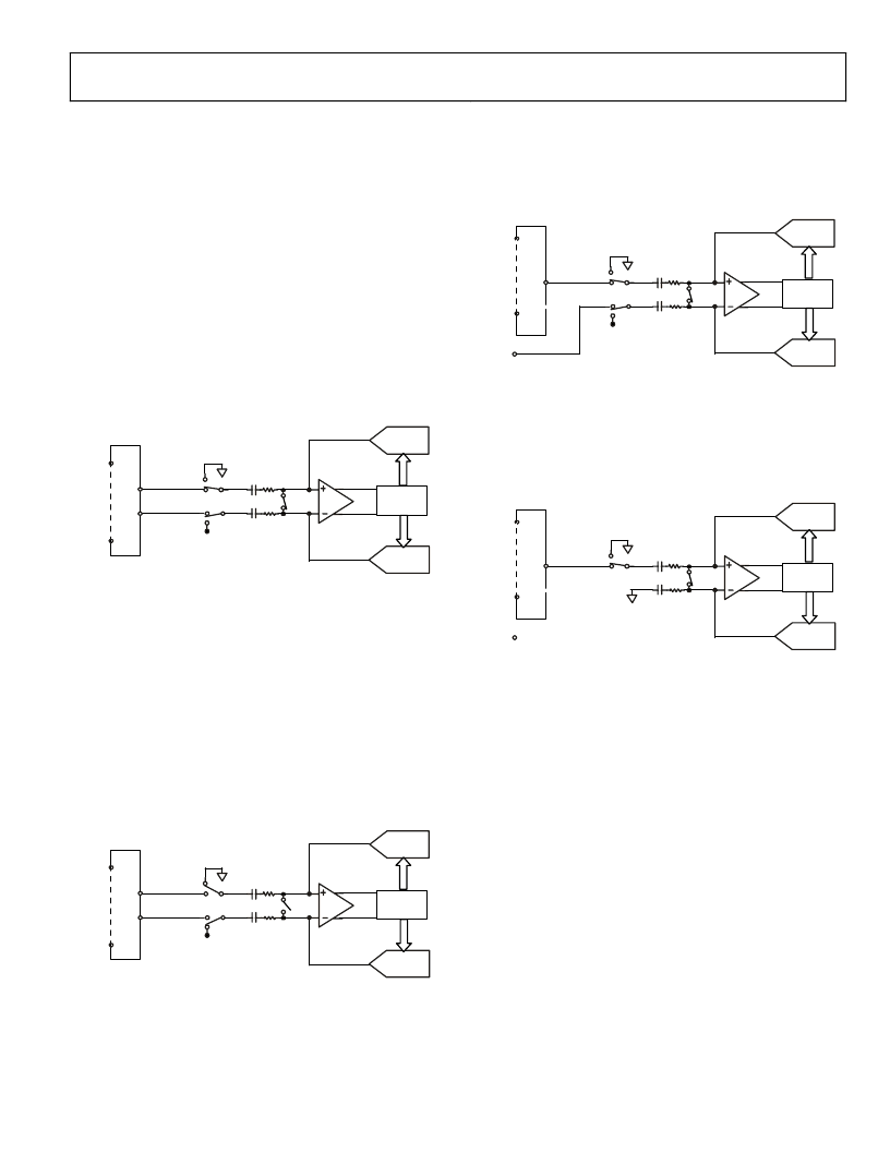
The ADC incorporates a successive approximation (SAR)
architecture involving a charge-sampled input stage. This
architecture is described below for the three different modes of
operation.
Differential mode
The ADuC702x contains a successive approximation ADC
based on two capacitive DACs. Figure 11 and Figure 12 show
simplified schematics of the ADC in acquisition and conversion
phase, respectively. The ADC is comprised of control logic, a
SAR, and two capacitive DACs. In Figure 11 (the acquisition
phase), SW3 is closed and SW1 and SW2 are in Position A, the
comparator is held in a balanced condition, and the sampling
capacitor arrays acquire the differential signal on the input.
Cs
Cs
A
B
A
B
Channel+
Channel-
CAPACITIVE
DAC
CAPACITIVE
DAC
MUX
CONTROL
LOGIC
COMPARATOR
AIN0
AIN11
.
SW3
SW2
SW1
V
REF
Figure 11: ADC acquisition phase
When the ADC starts a conversion (Figure 12), SW3 will open
and SW1 and SW2 will move to Position B, causing the
comparator to become unbalanced. Both inputs are
disconnected once the conversion begins. The control logic and
the charge redistribution DACs are used to add and subtract
fixed amounts of charge from the sampling capacitor arrays to
bring the comparator back into a balanced condition. When the
comparator is rebalanced, the conversion is complete. The
control logic generates the ADC’s output code. The output
impedances of the sources driving the V
IN+
and V
IN–
pins must
be matched; otherwise, the two inputs will have different
settling times, resulting in errors.
Cs
Cs
A
B
A
B
VREF
Channel+
Channel-
CAPACITIVE
DAC
CAPACITIVE
DAC
MUX
CONTROL
LOGIC
COMPARATOR
AIN0
AIN11
.
SW3
SW2
SW1
Figure 12: ADC conversion phase
Pseudo-differential mode
In pseudo-differential mode, Channel- is linked to the VIN- pin
of the ADuC702x and SW2 switches between A (Channel-) and
B (VREF). VIN- pin must be connected to Ground or a low
voltage. The input signal on V
IN
+ can then vary from V
IN
- to
V
REF
+ V
IN
-. Note V
IN
- must be chosen so that V
REF
+ V
IN
- does
not exceed AV
DD
.
Cs
Cs
A
B
A
B
Channel+
Channel-
CAPACITIVE
DAC
CAPACITIVE
DAC
MUX
CONTROL
LOGIC
COMPARATOR
AIN0
AIN11
.
SW3
SW2
SW1
V
REF
VIN-
Figure 13: ADC in pseudo-differential mode
Single-ended mode
In Single-ended mode, SW2 is always connected internally to
ground. The VIN- pin can be floating. The input signal range on
V
IN
+ is 0V to V
REF
.
Cs
Cs
A
B
Channel+
Channel-
CAPACITIVE
DAC
CAPACITIVE
DAC
MUX
CONTROL
LOGIC
COMPARATOR
AIN0
AIN11
.
SW3
SW1
VIN-
Figure 14: ADC in single-ended mode
Analog Input Structure
Figure 15 shows the equivalent circuit of the analog input
structure of the ADC. The four diodes provides ESD protection
for the analog inputs. Care must be taken to ensure that the
analog input signals never exceed the supply rails by more than
300 mV. This would cause these diodes to become forward
biased and start conducting into the substrate. These diodes can
conduct up to 10 mA without causing irreversible damage to
the part.
The capacitors C1 in Figure 15 are typically 4 pF and can
primarily be attributed to pin capacitance. The resistors are
lumped components made up of the ON resistance of the
switches. The value of these resistors is typically about 100
The capacitors, C2, are the ADC’s sampling capacitors and
have a capacitance of 16 pF typically.
.
For AC applications, removing high-frequency components
from the analog input signal is recommended by the use of an
RC low-pass filter on the relevant analog input pins. In
applications where harmonic distortion and signal-to-noise
相關PDF資料 |
PDF描述 |
|---|---|
| ADUC7025BCP32 | Precision Analog Microcontroller 12-bit Analog I/O, ARM7TDMI MCU |
| ADUC7025BCP62 | Precision Analog Microcontroller 12-bit Analog I/O, ARM7TDMI MCU |
| ADUC7026BST62 | Precision Analog Microcontroller 12-bit Analog I/O, ARM7TDMI MCU |
| ADUC7027AST62 | Precision Analog Microcontroller 12-bit Analog I/O, ARM7TDMI MCU |
| ADUC7027BST62 | Precision Analog Microcontroller 12-bit Analog I/O, ARM7TDMI MCU |
相關代理商/技術參數 |
參數描述 |
|---|---|
| ADUC7024BST62-U1 | 制造商:Analog Devices 功能描述: |
| ADUC7024BSTZ62 | 功能描述:IC MCU FLASH 62K ANLG I/O 64LQFP RoHS:是 類別:集成電路 (IC) >> 嵌入式 - 微控制器, 系列:MicroConverter® ADuC7xxx 標準包裝:38 系列:Encore!® XP® 核心處理器:eZ8 芯體尺寸:8-位 速度:5MHz 連通性:IrDA,UART/USART 外圍設備:欠壓檢測/復位,LED,POR,PWM,WDT 輸入/輸出數:16 程序存儲器容量:4KB(4K x 8) 程序存儲器類型:閃存 EEPROM 大小:- RAM 容量:1K x 8 電壓 - 電源 (Vcc/Vdd):2.7 V ~ 3.6 V 數據轉換器:- 振蕩器型:內部 工作溫度:-40°C ~ 105°C 封裝/外殼:20-SOIC(0.295",7.50mm 寬) 包裝:管件 其它名稱:269-4116Z8F0413SH005EG-ND |
| ADUC7024BSTZ62-RL | 功能描述:IC MCU 12BIT 1MSPS UART 64-LQFP RoHS:是 類別:集成電路 (IC) >> 嵌入式 - 微控制器, 系列:MicroConverter® ADuC7xxx 標準包裝:38 系列:Encore!® XP® 核心處理器:eZ8 芯體尺寸:8-位 速度:5MHz 連通性:IrDA,UART/USART 外圍設備:欠壓檢測/復位,LED,POR,PWM,WDT 輸入/輸出數:16 程序存儲器容量:4KB(4K x 8) 程序存儲器類型:閃存 EEPROM 大小:- RAM 容量:1K x 8 電壓 - 電源 (Vcc/Vdd):2.7 V ~ 3.6 V 數據轉換器:- 振蕩器型:內部 工作溫度:-40°C ~ 105°C 封裝/外殼:20-SOIC(0.295",7.50mm 寬) 包裝:管件 其它名稱:269-4116Z8F0413SH005EG-ND |
| ADUC7024HWEIZ-RL | 制造商:Analog Devices 功能描述: |
| ADuC7025 | 制造商:Analog Devices 功能描述: |
發布緊急采購,3分鐘左右您將得到回復。