- 您現在的位置:買賣IC網 > PDF目錄374044 > ADV3000-EVALZ (Analog Devices, Inc.) 3:1 HDMI/DVI Switch with Equalization PDF資料下載
參數資料
| 型號: | ADV3000-EVALZ |
| 廠商: | Analog Devices, Inc. |
| 英文描述: | 3:1 HDMI/DVI Switch with Equalization |
| 中文描述: | 3:1的HDMI / DVI接口與均衡開關 |
| 文件頁數: | 15/28頁 |
| 文件大小: | 608K |
| 代理商: | ADV3000-EVALZ |
第1頁第2頁第3頁第4頁第5頁第6頁第7頁第8頁第9頁第10頁第11頁第12頁第13頁第14頁當前第15頁第16頁第17頁第18頁第19頁第20頁第21頁第22頁第23頁第24頁第25頁第26頁第27頁第28頁
ADV3000
Rev. 0 | Page 15 of 28
START
FIXED PART
ADDR
REGISTER ADDR
FIXED PART
ADDR
DATA
STOP
ACK
I2C_ADDR0
ACK
R/W
ADDR
ACK
ACK
R/W
SR
1
2
3
4
5
6
7
8
9 10 11
12
13
I2C_SCL
GENERI2C_SDA
EXAMPLE
I2C_SDA
0
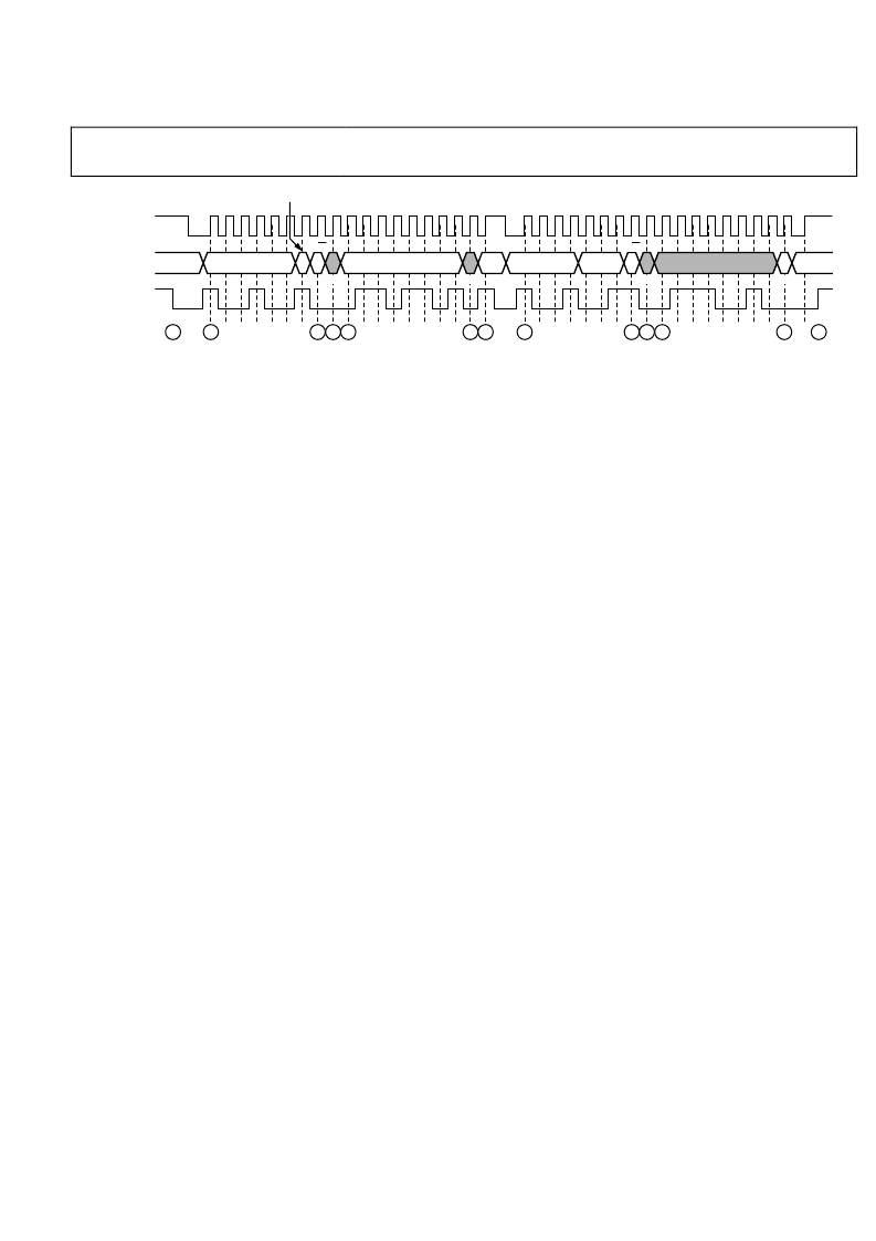
Figure 30. I
2
C Read Diagram
READ PROCEDURE
To read data from the ADV3000 register set, an I
2
C master
(such as a microcontroller) needs to send the appropriate
control signals to the ADV3000 slave device. The signals are
controlled by the I
2
C master, unless otherwise specified. For a
diagram of the procedure, see Figure 30. The steps for a read
procedure are as follows:
1.
Send a start condition (while holding the I2C_SCL line
high, pull the I2C_SDA line low).
2.
Send the ADV3000 part address (seven bits). The upper six
bits of the ADV3000 part address are the static value
[100100] and the LSB is set by Input Pin I2C_ADDR0. This
transfer should be MSB first.
3.
Send the write indicator bit (0).
4.
Wait for the ADV3000 to acknowledge the request.
5.
Send the register address (eight bits) from which data is to
be read. This transfer should be MSB first.
6.
Wait for the ADV3000 to acknowledge the request.
7.
Send a repeated start condition (Sr) by holding the
I2C_SCL line high and pulling the I2C_SDA line low.
8.
Resend the ADV3000 part address (seven bits) from Step 2.
The upper six bits of the ADV3000 part address are the
static value [100100] and the LSB is set by the Input Pin
I2C_ADDR0. This transfer should be MSB first.
9.
Send the read indicator bit (1).
10.
Wait for the ADV3000 to acknowledge the request.
11.
The ADV3000 serially transfers the data (eight bits) held in
the register indicated by the address set in Step 5. This data
is sent MSB first.
12.
Acknowledge the data from the ADV3000.
13.
Perform one of the following:
13a.
S
line high, pull the SDA line high) and release control
of the bus to end the transaction (shown in
13b.
ted start condition (while holding the
Send a repea
I2C_SCL line high, pull the I2C_SDA line low) and
continue with Step 2 of the write procedure (previous
Write Procedure section) to perform a write.
Send a repeated start condition (while holding the
I2C_SCL line high, pull the I2C_SDA line low) and
continue with Step 2 of this procedure to perform a
read from another address.
Send a repeated start conditi
I2C_SCL line high, pull the I2C_SDA line low) and
continue with Step 8 of this procedure to perform a
read from the same address.
ING/UPDATE DELAY
There is a delay between when a user
tion registers of the ADV3000 and when that state change take
physical effect. This update delay occurs regardless of whether
the user programs the ADV3000 via the serial or the parallel
control interface. When using the serial control interface, the
update delay begins at the falling edge of I2C_SCL for the last
data bit transferred, as shown in Figure 29. When using the
parallel control interface, the update delay begins at the
transition edge of the relevant parallel interface pin. This
delay is register specific and the times are specified in Table 1.
During a delay window, new values can be written to the
configuration registers, but the ADV3000 does not physic
update until the end of the delay window of that register. Writing
new values during the delay window does not reset the window;
new values supersede the previously written values. At the end
of the delay window, the ADV3000 physically assumes the state
indicated by the last set of values written to the configuration
registers. If the configuration registers are written after the dela
window ends, the ADV3000 immediately updates and a new
delay window begins.
op condition (while holding the I2C_SCL
end a st
).
13c.
13d.
on (while holding the
SWITCH
writes to the configura-
s
update
ally
y
Figure 30
相關PDF資料 |
PDF描述 |
|---|---|
| ADV453 | Circular Connector; No. of Contacts:22; Series:LJTP02R; Body Material:Aluminum; Connecting Termination:Crimp; Connector Shell Size:13; Circular Contact Gender:Socket; Circular Shell Style:Box Mount Receptacle |
| ADV458 | Triple 8-Bit Video RAM-DAC(三通道,8位視頻RAM-D/A轉換器) |
| ADV476KP35 | CMOS Monolithic 256x18 Color Palette RAM-DAC |
| ADV476KP50 | CMOS Monolithic 256x18 Color Palette RAM-DAC |
| ADV476KP66 | CMOS Monolithic 256x18 Color Palette RAM-DAC |
相關代理商/技術參數 |
參數描述 |
|---|---|
| ADV3002 | 制造商:AD 制造商全稱:Analog Devices 功能描述:4:1 HDMI/DVI Switch with Equalization, DDC/CEC Buffers and EDID Replication |
| ADV3002BSTZ | 功能描述:IC SWITCH HDMI/DVI 4:1 80LQFP RoHS:是 類別:集成電路 (IC) >> 接口 - 模擬開關,多路復用器,多路分解器 系列:- 應用說明:Ultrasound Imaging Systems Application Note 產品培訓模塊:Lead (SnPb) Finish for COTS Obsolescence Mitigation Program 標準包裝:250 系列:- 功能:開關 電路:單刀單擲 導通狀態電阻:48 歐姆 電壓電源:單電源 電壓 - 電源,單路/雙路(±):2.7 V ~ 5.5 V 電流 - 電源:5µA 工作溫度:0°C ~ 70°C 安裝類型:表面貼裝 封裝/外殼:48-LQFP 供應商設備封裝:48-LQFP(7x7) 包裝:托盤 |
| ADV3002BSTZ-RL | 功能描述:IC SWITCH HDMI/DVI 4:1 80-LQFP RoHS:是 類別:集成電路 (IC) >> 接口 - 模擬開關,多路復用器,多路分解器 系列:- 其它有關文件:STG4159 View All Specifications 標準包裝:5,000 系列:- 功能:開關 電路:1 x SPDT 導通狀態電阻:300 毫歐 電壓電源:雙電源 電壓 - 電源,單路/雙路(±):±1.65 V ~ 4.8 V 電流 - 電源:50nA 工作溫度:-40°C ~ 85°C 安裝類型:表面貼裝 封裝/外殼:7-WFBGA,FCBGA 供應商設備封裝:7-覆晶 包裝:帶卷 (TR) |
| ADV3002-EVALZ | 制造商:AD 制造商全稱:Analog Devices 功能描述:4:1 HDMI/DVI Switch with Equalization, DDC/CEC Buffers and EDID Replication |
| ADV3002XSTZ | 功能描述:IC SWITCH HDMI/DVI 4:1 80LQFP 制造商:analog devices inc. 系列:- 包裝:托盤 零件狀態:上次購買時間 類型:視頻開關 應用:HDTV,投影儀,機頂盒 安裝類型:- 封裝/外殼:- 供應商器件封裝:- 標準包裝:1 |
發布緊急采購,3分鐘左右您將得到回復。