- 您現在的位置:買賣IC網 > PDF目錄374044 > ADV601JS (ANALOG DEVICES INC) Low Cost Multiformat Video Codec PDF資料下載
參數資料
| 型號: | ADV601JS |
| 廠商: | ANALOG DEVICES INC |
| 元件分類: | 消費家電 |
| 英文描述: | Low Cost Multiformat Video Codec |
| 中文描述: | SPECIALTY CONSUMER CIRCUIT, PQFP160 |
| 封裝: | PLASTIC, QFP-160 |
| 文件頁數: | 37/52頁 |
| 文件大小: | 606K |
| 代理商: | ADV601JS |
第1頁第2頁第3頁第4頁第5頁第6頁第7頁第8頁第9頁第10頁第11頁第12頁第13頁第14頁第15頁第16頁第17頁第18頁第19頁第20頁第21頁第22頁第23頁第24頁第25頁第26頁第27頁第28頁第29頁第30頁第31頁第32頁第33頁第34頁第35頁第36頁當前第37頁第38頁第39頁第40頁第41頁第42頁第43頁第44頁第45頁第46頁第47頁第48頁第49頁第50頁第51頁第52頁
ADV601
–37–
REV. 0
TIMING PARAMETERS
This section contains signal timing information for the ADV601. Timing descriptions for the following items appear in this
section:
Clock signal timing
Video data transfer timing (CCIR-656, Gray Scale/Philips, and Multiplexed Philips formats)
Host data transfer timing (direct register read/write access)
DSP data transfer (serial data transfer)
Clock Signal Timing
The diagram in this section shows timing for VCLK input and VCLKO output. All output values assume a maximum pin
loading of 50 pF.
Table XX. Video Clock Period, Frequency, Drift and Jitter
Min VCLK_CYC
Period
Nominal VCLK_CYC
Period (Frequency)
Max VCLK_CYC
Period
1, 2
Video Format
CCIR-601 PAL
Square Pixel PAL
CCIR-601 NTSC
Square Pixel NTSC
35.2 ns
32.2 ns
35.2 ns
38.7 ns
37 ns (27 MHz)
33.89 ns (29.5 MHz)
37 ns (27 MHz)
40.75 ns (24.54 MHz)
38.9 ns
35.5 ns
38.9 ns
42.7 ns
NOTES
1
VCLK Period Drift =
±
0.1 (VCLK_CYC/field.
2
VCLK edge-to-edge jitter = 1 ns.
Table XXI. Video Clock Duty Cycle
Min
Nominal
Max
VCLK Duty Cycle
1
(40%)
(50%)
(60%)
NOTE
1
VCLK Duty Cyle = t
VCLK_HI
/(t
VCLK_LO
)
×
100.
Table XXII. Video Clock Timing Parameters
Parameter
Description
Min
Max
Unit
t
VCLK_CYC
t
VCLKO_D0
t
VCLKO_D1
VCLK Signal, Cycle Time (1/Frequency) at 27 MHz
VCLKO Signal, Delay (when VCLK2 = 0) at 27 MHz
VCLKO Signal, Delay (when VCLK2 = 1) at 27 MHz
(See Video Clock Period Table)
10
10
29
29
ns
ns
TEST CONDITIONS
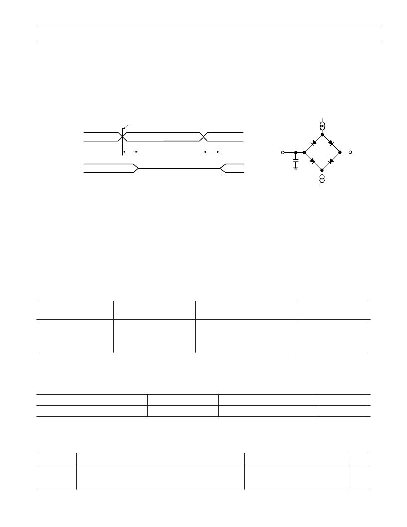
Figure 23 shows test condition voltage reference and device
loading information. These test conditions consider an output
as
disabled
when the output stops driving and goes from the
measured high or low voltage to a high impedance state. Tests
measure output disable time (t
DISABLE
) as the time between the
reference input signal crossing +1.5 V and the time that the
output reaches the high impedance state (also +1.5 V). Simi-
larly, these tests conditions consider an output as
enabled
when
the output leaves the high impedance state and begins driving a
measured high or low voltage. Tests measure output enable time
(t
ENABLE
) as the time between the reference input signal crossing
+1.5 V and the time that the output reaches the measured high
or low voltage.
INPUT
REFERENCE
SIGNAL
OUTPUT
SIGNAL
t
DISABLED
t
ENABLED
1.5V
V
OH
V
OL
V
IH
V
IL
1.5V
INPUT & OUTPUT VOLTAGE/TIMING REFERENCES
DEVICE LOADING FOR AC MEASUREMENTS
TO
OUTPIN
2pF
+1.5V
I
OL
I
OH
Figure 23. Test Condition Voltage Reference and Device Loading
相關PDF資料 |
PDF描述 |
|---|---|
| ADV601LC | Ultralow Cost Video Codec |
| ADV601LCJST | Ultralow Cost Video Codec |
| ADV7120KP30 | CMOS 80 MHz, Triple 8-Bit Video DAC |
| ADV7120 | CMOS 80 MHz, Triple 8-Bit Video DAC |
| ADV7120KP50 | CMOS 80 MHz, Triple 8-Bit Video DAC |
相關代理商/技術參數 |
參數描述 |
|---|---|
| ADV601JS12 | 制造商:Analog Devices 功能描述:Multiformat Video Codec 160-Pin MQFP 制造商:Rochester Electronics LLC 功能描述:DIGITAL VIDEO CODEC REV 1.2 - Bulk |
| ADV601LC | 制造商:AD 制造商全稱:Analog Devices 功能描述:Ultralow Cost Video Codec |
| ADV601LCERAG1266B-0.5 | 制造商:Analog Devices 功能描述: |
| ADV601LCJST | 制造商:Analog Devices 功能描述:Ultralow Cost Video Codec 120-Pin LQFP 制造商:Analog Devices 功能描述:IC VIDEO CODEC |
| ADV601LCJSTRL | 制造商:Analog Devices 功能描述:Ultralow Cost Video Codec 120-Pin LQFP T/R |
發布緊急采購,3分鐘左右您將得到回復。