- 您現在的位置:買賣IC網 > PDF目錄374045 > ADV7127KR50 (ANALOG DEVICES INC) CMOS, 240 MHz 10-Bit High Speed Video DAC PDF資料下載
參數資料
| 型號: | ADV7127KR50 |
| 廠商: | ANALOG DEVICES INC |
| 元件分類: | DAC |
| 英文描述: | CMOS, 240 MHz 10-Bit High Speed Video DAC |
| 中文描述: | PARALLEL, WORD INPUT LOADING, 10-BIT DAC, PDSO28 |
| 封裝: | SOIC-28 |
| 文件頁數: | 12/16頁 |
| 文件大小: | 307K |
| 代理商: | ADV7127KR50 |
ADV7127
–12–
REV. 0
CIRCUIT DESCRIPTION AND OPERATION
The ADV7127 contains one 10-bit D/A converter, with one
input channel containing a 10-bit register. A reference amplifier
is also integrated on board the part.
Digital Inputs
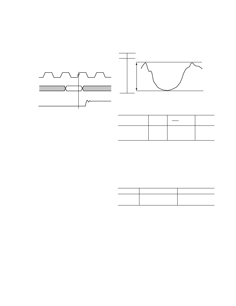
Ten bits of data (color information) D0–D9 are latched into the
device on the rising edge of each clock cycle. This data is pre-
sented to the 10-bit DAC and is then converted to an analog
output waveform. See Figure 20.
CLOCK
DATA
ANALOG OUTPUTS
, I
OUT
DIGITAL INPUTS
D0–D9
I
OUT
Figure 20.Video Data Input/Output
All these digital inputs are specified to accept TTL logic levels.
Clock Input
The CLOCK input of the ADV7127 is typically the pixel clock
rate of the system. It is also known as the dot rate. The dot rate,
and hence the required CLOCK frequency, will be determined
by the on-screen resolution, according to the following equation:
Dot Rate
= (
Horiz Res
)
×
(
Vert Res
)
×
(
Refresh Rate
)/
(
Retrace Factor
)
Horiz Res
= Number of Pixels/Line.
Vert Res
= Number of Lines/Frame.
Refresh Rate
= Horizontal Scan Rate. This is the rate at
which the screen must be refreshed, typically
60 Hz for a noninterlaced system or 30 Hz
for an interlaced system.
Retrace Factor
= Total Blank Time Factor. This takes into
account that the display is blanked for a
certain fraction of the total duration of each
frame (e.g., 0.8).
Therefore, if we have a graphics system with
a 1024
×
1024 resolution, a noninterlaced
60 Hz refresh rate and a retrace factor of 0.8,
then:
Dot Rate
= 1024
×
1024
×
60/0.8
= 78.6 MHz
The required CLOCK frequency is thus 78.6 MHz.
All video data and control inputs are latched into the ADV7127
on the rising edge of CLOCK, as previously described in the
Digital Inputs section. It is recommended that the CLOCK
input to the ADV7127 be driven by a TTL buffer (e.g., 74F244).
I
OUT
mA
V
17.61
0.66
0
0
BLACK
LEVEL
WHITE
LEVEL
100 IRE
Figure 21. I
OUT
Video Output Waveform
Table I. Video Output Truth Table (RSET = 560
V
,
R
LOAD
= 37.5
V
)
Description
Data
DAC
Input
I
OUT
I
OUT
WHITE LEVEL
VIDEO
BLACK LEVEL
17.62
Video
0
0
17.62 – Video
17.62
3FF
Data
000H
Power Management
The
PSAVE
input of the ADV7127 puts the part into standby
mode. It is used to reduce power consumption. When
PSAVE
is low, the power may be reduced to approximately 10 mW at
3 V. The ADV7127 in TSSOP package also has a power-down
feature where the entire part, including the voltage reference
circuit, is powered down. In this case, power on the ADV7127
can be reduced to 60
μ
W at 3 V.
Table II. Power Management
Mode
ADV7127 TSSOP
ADV7127 SOIC
Power-Save
Power-Down Power 60
μ
W at 3 V
10 mW Typically at 3 V 10 mW Typically at 3 V
Not Available
Reference Input
The ADV7127 has an on-board voltage reference. The V
REF
pin is normally terminated to V
AA
through a 0.1
μ
F capacitor.
Alternatively, the part could, if required, be overdriven by an
external 1.23 V reference (AD1580).
A resistance R
SET
connected between the R
SET
pin and GND
determines the amplitude of the output video level according to
the following equation:
I
OUT
(mA) =
7,968
×
V
REF
(V)/R
SET
(
)
Using a variable value of R
SET
, as shown in Figure 22, allows
for accurate adjustment of the analog output video levels. Use
of a fixed 560
R
SET
resistor yields the analog output levels
as quoted in the specification page. These values typically
correspond to the RS-343A video waveform values as shown in
Figure 21.
(1)
相關PDF資料 |
PDF描述 |
|---|---|
| ADV7127KRU50 | CMOS, 240 MHz 10-Bit High Speed Video DAC |
| ADV7127KRU140 | CMOS, 240 MHz 10-Bit High Speed Video DAC |
| ADV7127JRU240 | CMOS, 240 MHz 10-Bit High Speed Video DAC |
| ADV7127 | CMOS, 240 MHz 10-Bit High Speed Video DAC |
| ADV7127JR240 | CMOS, 240 MHz 10-Bit High Speed Video DAC |
相關代理商/技術參數 |
參數描述 |
|---|---|
| ADV7127KR50-REEL | 制造商:Analog Devices 功能描述:DAC 1-CH Segment 10-bit 28-Pin SOIC W T/R 制造商:Rochester Electronics LLC 功能描述:SINGLE HIGH SPEED VIDEO DAC I.C. - Tape and Reel |
| ADV7127KRU140 | 功能描述:IC DAC VID 140MHZ 3.3/5V 24TSSOP RoHS:否 類別:集成電路 (IC) >> 數據采集 - 數模轉換器 系列:- 產品培訓模塊:Data Converter Fundamentals DAC Architectures 標準包裝:750 系列:- 設置時間:7µs 位數:16 數據接口:并聯 轉換器數目:1 電壓電源:雙 ± 功率耗散(最大):100mW 工作溫度:0°C ~ 70°C 安裝類型:表面貼裝 封裝/外殼:28-LCC(J 形引線) 供應商設備封裝:28-PLCC(11.51x11.51) 包裝:帶卷 (TR) 輸出數目和類型:1 電壓,單極;1 電壓,雙極 采樣率(每秒):143k |
| ADV7127KRU50 | 功能描述:IC DAC VIDEO SGL HI SPD 24-TSSOP RoHS:否 類別:集成電路 (IC) >> 數據采集 - 數模轉換器 系列:- 標準包裝:47 系列:- 設置時間:2µs 位數:14 數據接口:并聯 轉換器數目:1 電壓電源:單電源 功率耗散(最大):55µW 工作溫度:-40°C ~ 85°C 安裝類型:表面貼裝 封裝/外殼:28-SSOP(0.209",5.30mm 寬) 供應商設備封裝:28-SSOP 包裝:管件 輸出數目和類型:1 電流,單極;1 電流,雙極 采樣率(每秒):* |
| ADV7127KRU50-REEL | 功能描述:IC DAC VIDEO 50MHZ 3.3/5 24TSSOP RoHS:否 類別:集成電路 (IC) >> 數據采集 - 數模轉換器 系列:- 標準包裝:47 系列:- 設置時間:2µs 位數:14 數據接口:并聯 轉換器數目:1 電壓電源:單電源 功率耗散(最大):55µW 工作溫度:-40°C ~ 85°C 安裝類型:表面貼裝 封裝/外殼:28-SSOP(0.209",5.30mm 寬) 供應商設備封裝:28-SSOP 包裝:管件 輸出數目和類型:1 電流,單極;1 電流,雙極 采樣率(每秒):* |
| ADV7127KRUZ140 | 功能描述:IC DAC VID 140MHZ 3.3/5V 24TSSOP RoHS:是 類別:集成電路 (IC) >> 數據采集 - 數模轉換器 系列:- 產品培訓模塊:Lead (SnPb) Finish for COTS Obsolescence Mitigation Program 標準包裝:50 系列:- 設置時間:4µs 位數:12 數據接口:串行 轉換器數目:2 電壓電源:單電源 功率耗散(最大):- 工作溫度:-40°C ~ 85°C 安裝類型:表面貼裝 封裝/外殼:8-TSSOP,8-MSOP(0.118",3.00mm 寬) 供應商設備封裝:8-uMAX 包裝:管件 輸出數目和類型:2 電壓,單極 采樣率(每秒):* 產品目錄頁面:1398 (CN2011-ZH PDF) |
發布緊急采購,3分鐘左右您將得到回復。