- 您現在的位置:買賣IC網 > PDF目錄374045 > ADV7152LS110 (ANALOG DEVICES INC) CMOS 220 MHz True-Color Graphics Triple 10-Bit Video RAM-DAC PDF資料下載
參數資料
| 型號: | ADV7152LS110 |
| 廠商: | ANALOG DEVICES INC |
| 元件分類: | 顯示控制器 |
| 英文描述: | CMOS 220 MHz True-Color Graphics Triple 10-Bit Video RAM-DAC |
| 中文描述: | PALETTE-DAC DSPL CTLR, PQFP100 |
| 封裝: | PLASTIC, QFP-100 |
| 文件頁數: | 11/32頁 |
| 文件大小: | 454K |
| 代理商: | ADV7152LS110 |
第1頁第2頁第3頁第4頁第5頁第6頁第7頁第8頁第9頁第10頁當前第11頁第12頁第13頁第14頁第15頁第16頁第17頁第18頁第19頁第20頁第21頁第22頁第23頁第24頁第25頁第26頁第27頁第28頁第29頁第30頁第31頁第32頁
ADV7152
–11–
REV. B
Color data is latched into the parts pixel port on every rising
edge of L OADIN (see T iming Waveform, Figure 3). T he
required frequency of LOADIN is determined by the multiplex
rate, where
f
LOADIN
= f
CLOCK
/2
2:1 Multiplex Mode
f
LOADIN
= f
CLOCK
1:1 Multiplex Mode
Other pixel data signals latched into the device by LOADIN
include
SYNC
,
BLANK
and PS0–PS1.
Internally, data is pipelined through the part by the differential
pixel clock inputs, CLOCK and
CLOCK
. T he LOADIN con-
trol signal needs only have a frequency synchronous relationship
to the pixel CLOCK (see “Pipeline Delay & Onboard Calibra-
tion” section). A completely phase independent LOADIN signal
can be used with the ADV7152, allowing the CLOCK to occur
anywhere during the LOADIN cycle.
Alternatively, the LOADOUT signal of the ADV7152 can be
used. LOADOUT can be connected either directly or indirectly
to LOADIN. Its frequency is automatically set to the correct
LOADIN requirement.
SYNC
,
BLANK
T he
BLANK
and
SYNC
video control signals drive the analog
outputs to the blanking and
SYNC
levels respectively. T hese
signals are latched into the part on the rising edge of LOADIN.
T he
SYNC
information is encoded onto the IOG analog signal
when bit CR22 of Command Register 2 is set to a Logic “1.”
T he
SYNC
input is ignored if CR22 is set to “0.”
SYNCOUT
In some applications where it is not permissible to encode
SYNC
on green (IOG),
SYNCOUT
can be used as a separate
T T L digital
SYNC
output. T his has the advantage over an inde-
pendent (of the ADV7150)
SYNC
in that it does not necessitate
knowing the absolute pipeline delay of the part. T his allows
complete independence between LOADIN/Pixel Data and
CLOCK . T he
SYNC
input is connected to the device as normal
with Bit CR22 of Command Register 2 set to “0” thereby pre-
venting
SYNC
from being encoded onto IOG. Bit CR12 of
Command Register 1 is set to “1,” enabling
SYNCOUT
. T he
output signal generates a T T L
SYNCOUT
with correct pipeline
delay that is capable of directly driving the composite
SYNC
signal of a computer monitor.
PS0–PS1 (Palette Priority Select Inputs)
T hese pixel port select inputs determine whether or not the de-
vice is selected. T hese controls effectively determine whether the
devices RGB analog outputs are turned-on or shut down. When
the analog outputs are shut down, IOR, IOG and IOB are
forced to 0 mA regardless of the state of the pixel and control
data inputs. T his state is determined on a pixel by pixel basis as
the PS0–PS1 inputs are multiplexed in exactly the same format
as the pixel port color data. T hese controls allow for switching
between multiple palette devices (see Appendix 4). If the values
of PS0 and PSI match the values programmed into bits MR16
and MR17 of the Mode Register, then the device is selected, if
there is no match the device is effectively shut down.
Multiplexing
T he onboard multiplexers of the ADV7152 eliminate the need
for external data serializer circuits. Multiple video memory de-
vices can be connected, in parallel, directly to the device. Fig-
ure 11 shows two memory banks of 50 MHz memory connected
to the ADV7152, running in 2:1 multiplex mode, giving a
resultant pixel or dot clock rate of 100 MHz. As mentioned in
the previous section, the ADV7152 supports a number of color
data formats in 2:1 and 1:1 multiplex modes.
In 1:1 multiplex mode, the ADV7152 is clocked using the
LOADIN signal. T his means that there is no requirement for
differential ECL inputs on CLOCK and
CLOCK
. T he pixel
clock is connected directly to L OADIN. (Note: T he ECL
C LOCK can still be used to generate LOADOUT PRGCK OUT ,
etc.)
VRAM (BANK A)
VRAM (BANK B)
MULTIPLEXER
24
24
24
ADV7152
VIDEO MEMORY/
FRAME BUFFER
100MHz
(2 x 50MHz)
50MHz
50MHz
A
B
Figure 11. Direct Interfacing of Video Memory to
ADV7152
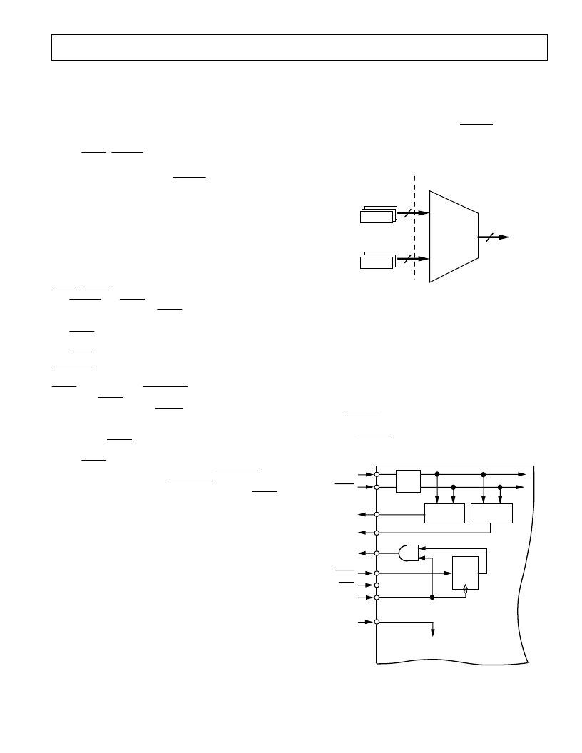
CLOCK CONT ROL CIRCUIT
T he ADV7152 has an integrated Clock Control Circuit (Figure
12). T his circuit is capable of both generating the ADV7152’s
internal clocking signals as well as external graphics subsystem
clocking signals. T otal system synchronization can be attained
by using the parts output clocking signals to drive the control-
ling graphics processor’s master clock as well as the video frame
buffers shift clock signals.
CLOCK ,
CLOCK
Inputs
T he Clock Control Circuit is driven by the pixel clock inputs,
CLOCK and
CLOCK
. T hese inputs can be driven by a differ-
ential ECL oscillator running from a +5 V supply.
CLOCK
ADV7152
CLOCK
DIVIDE BY N
(
÷
N)
LOADOUT
DIVIDE BY M
(
÷
M)
PRGCKOUT
LOADIN
SCKOUT
SCKIN
BLANK
LATCH
ENABLE
SYNC
TO COLOR DATA
MULTIPLEXER
ECL
TO
TTL
M IS A FUNCTION OF MULTIPLEX RATE
M = 2 IN 2:1 MULTIPLEX MODE
M = 1 IN 1:1 MULTIPLEX MODE
N IS INDEPENDENTLY
PROGRAMMABLE
N= (4, 8, 16, 32)
Figure 12. Clock Control Circuit of the ADV7152
相關PDF資料 |
PDF描述 |
|---|---|
| ADV7152LS135 | CMOS 220 MHz True-Color Graphics Triple 10-Bit Video RAM-DAC |
| ADV7152LS170 | CMOS 220 MHz True-Color Graphics Triple 10-Bit Video RAM-DAC |
| ADV7152LS220 | CMOS 220 MHz True-Color Graphics Triple 10-Bit Video RAM-DAC |
| ADV7160 | 96-Bit, 220 MHz True-Color Video RAM-DAC(96位,220MHz,真彩色視頻RAM-D/A轉換器) |
| ADV7162 | 96-Bit, 220 MHz True-Color Video RAM-DAC(96位,220MHz,真彩色視頻RAM-D/A轉換器) |
相關代理商/技術參數 |
參數描述 |
|---|---|
| ADV7152LS135 | 制造商:Rochester Electronics LLC 功能描述:- Bulk |
| ADV7152LS170 | 制造商:AD 制造商全稱:Analog Devices 功能描述:CMOS 220 MHz True-Color Graphics Triple 10-Bit Video RAM-DAC |
| ADV7152LS220 | 制造商:Analog Devices 功能描述: 制造商:Analog Devices 功能描述:PALETTE-DAC DSPL CTLR, PQFP100 |
| ADV7152LS85 | 制造商:AD 制造商全稱:Analog Devices 功能描述:CMOS 220 MHz True-Color Graphics Triple 10-Bit Video RAM-DAC |
| ADV7160 | 制造商:AD 制造商全稱:Analog Devices 功能描述:96-Bit, 220 MHz True-Color Video RAM-DAC |
發布緊急采購,3分鐘左右您將得到回復。