- 您現在的位置:買賣IC網 > PDF目錄374046 > ADV7170KS (ANALOG DEVICES INC) Digital PAL/NTSC Video Encoder with 10-Bit SSAF⑩ and Advanced Power Management PDF資料下載
參數資料
| 型號: | ADV7170KS |
| 廠商: | ANALOG DEVICES INC |
| 元件分類: | 顏色信號轉換 |
| 英文描述: | Digital PAL/NTSC Video Encoder with 10-Bit SSAF⑩ and Advanced Power Management |
| 中文描述: | COLOR SIGNAL ENCODER, PQFP44 |
| 封裝: | MS-022AB, MQFP-44 |
| 文件頁數: | 27/55頁 |
| 文件大小: | 754K |
| 代理商: | ADV7170KS |
第1頁第2頁第3頁第4頁第5頁第6頁第7頁第8頁第9頁第10頁第11頁第12頁第13頁第14頁第15頁第16頁第17頁第18頁第19頁第20頁第21頁第22頁第23頁第24頁第25頁第26頁當前第27頁第28頁第29頁第30頁第31頁第32頁第33頁第34頁第35頁第36頁第37頁第38頁第39頁第40頁第41頁第42頁第43頁第44頁第45頁第46頁第47頁第48頁第49頁第50頁第51頁第52頁第53頁第54頁第55頁
ADV7170/ADV7171
–27–
REV. 0
TR0 BIT DESCRIPTION
Master/Slave Control (TR00)
This bit controls whether the ADV7170/ADV7171 is in master
or slave mode.
Timing Mode Control (TR02–TR01)
These bits control the timing mode of the ADV7170/ADV7171.
These modes are described in more detail in the Timing and
Control section of the data sheet.
BLANK
Control (TR03)
This bit controls whether the
BLANK
input is used when the
part is in slave mode.
Luma Delay Control (TR05–TR04)
These bits control the addition of a luminance delay. Each bit
represents a delay of 74 ns.
Pixel Port Select (TR06)
This bit is used to set the pixel port to accept 8-bit or 16-bit
data. If an 8-bit input is selected the data will be set up on Pins
P7–P0.
Timing Register Reset (TR07)
Toggling TR07 from low to high and low again resets the inter-
nal timing counters. This bit should be toggled after power-up,
reset or changing to a new timing mode.
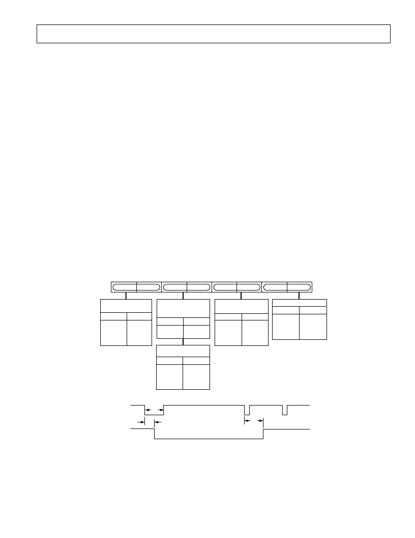
TR11
TR10
TR17
TR12
TR13
TR15
TR16
TR14
HSYNC
TO PIXEL
DATA ADJUSTMENT
TR17 TR16
0
0
1
1
0
1
0
1
0
3
T
PCLK
1
3
T
PCLK
2
3
T
PCLK
3
3
T
PCLK
HSYNC
TO
FIELD/
VSYNC
DELAY
TR13 TR12
0
0
1
1
0
1
0
1
0
3
T
PCLK
4
3
T
PCLK
8
3
T
PCLK
16
3
T
PCLK
T
B
HSYNC
WIDTH
0
0
1
1
0
1
0
1
1
3
T
PCLK
4
3
T
PCLK
16
3
T
PCLK
128
3
T
PCLK
TR11 TR10
T
A
HSYNC
TO FIELD
RISING EDGE DELAY
(MODE 1 ONLY)
x
x
0
1
T
B
T
B
+ 32
m
s
TR15 TR14
T
C
VSYNC
WIDTH
(MODE 2 ONLY)
TR15 TR14
0
0
1
1
0
1
0
1
1
3
T
PCLK
4
3
T
PCLK
16
3
T
PCLK
128
3
T
PCLK
LINE 313
LINE 314
LINE 1
T
B
TIMING MODE 1 (MASTER/PAL)
HSYNC
FIELD/
VSYNC
T
A
T
C
Figure 44. Timing Register 1
TIMING REGISTER 1 (TR17–TR10)
(Address (SR4–SR0) = 08H)
Timing Register 1 is a 8-bit-wide register.
Figure 44 shows the various operations under the control of
Timing Register 1. This register can be read from as well writ-
ten to. This register can be used to adjust the width and position
of the master mode timing signals.
TR1 BIT DESCRIPTION
HSYNC
Width (TR11–TR10)
These bits adjust the
HSYNC
pulsewidth.
HSYNC
to
VSYNC
/FIELD Delay Control (TR13–TR12)
These bits adjust the position of the
HSYNC
output relative to
the FIELD/
VSYNC
output.
HSYNC
to FIELD Delay Control (TR15–TR14)
When the ADV7170/ADV7171 is in timing mode 1, these bits
adjust the position of the
HSYNC
output relative to the FIELD
output rising edge.
VSYNC
Width (TR15–TR14)
When the ADV7170/ADV7171 is configured in Timing Mode
2, these bits adjust the
VSYNC
pulsewidth.
HSYNC
to Pixel Data Adjust (TR17–TR16)
This enables the
HSYNC
to be adjusted with respect to the
pixel data. This allows the Cr and Cb components to be
swapped. This adjustment is available in both master and slave
timing modes.
相關PDF資料 |
PDF描述 |
|---|---|
| ADV7170SU | Digital PAL/NTSC Video Encoder with 10-Bit SSAF⑩ and Advanced Power Management |
| ADV7171KS | Digital PAL/NTSC Video Encoder with 10-Bit SSAF⑩ and Advanced Power Management |
| ADV7171SU | Digital PAL/NTSC Video Encoder with 10-Bit SSAF⑩ and Advanced Power Management |
| ADV7171* | Digital PAL/NTSC Video Encoder with 10-Bit SSAF and Advanced Power Management |
| ADV7171 | Digital PAL/NTSC Video Encoder(數字PAL/NTSC視頻編碼器) |
相關代理商/技術參數 |
參數描述 |
|---|---|
| ADV7170KSUZ | 制造商:AD 制造商全稱:Analog Devices 功能描述:Digital PAL/NTSC Video Encoder |
| ADV7170KSUZ-REEL | 制造商:AD 制造商全稱:Analog Devices 功能描述:Digital PAL/NTSC Video Encoder |
| ADV7170KSZ | 制造商:AD 制造商全稱:Analog Devices 功能描述:Digital PAL/NTSC Video Encoder |
| ADV7170KSZ-REEL | 制造商:AD 制造商全稱:Analog Devices 功能描述:Digital PAL/NTSC Video Encoder |
| ADV7170SU | 制造商:AD 制造商全稱:Analog Devices 功能描述:Digital PAL/NTSC Video Encoder with 10-Bit SSAF⑩ and Advanced Power Management |
發布緊急采購,3分鐘左右您將得到回復。