- 您現在的位置:買賣IC網 > PDF目錄374046 > ADV7170KS (ANALOG DEVICES INC) Digital PAL/NTSC Video Encoder with 10-Bit SSAF⑩ and Advanced Power Management PDF資料下載
參數資料
| 型號: | ADV7170KS |
| 廠商: | ANALOG DEVICES INC |
| 元件分類: | 顏色信號轉換 |
| 英文描述: | Digital PAL/NTSC Video Encoder with 10-Bit SSAF⑩ and Advanced Power Management |
| 中文描述: | COLOR SIGNAL ENCODER, PQFP44 |
| 封裝: | MS-022AB, MQFP-44 |
| 文件頁數: | 29/55頁 |
| 文件大小: | 754K |
| 代理商: | ADV7170KS |
第1頁第2頁第3頁第4頁第5頁第6頁第7頁第8頁第9頁第10頁第11頁第12頁第13頁第14頁第15頁第16頁第17頁第18頁第19頁第20頁第21頁第22頁第23頁第24頁第25頁第26頁第27頁第28頁當前第29頁第30頁第31頁第32頁第33頁第34頁第35頁第36頁第37頁第38頁第39頁第40頁第41頁第42頁第43頁第44頁第45頁第46頁第47頁第48頁第49頁第50頁第51頁第52頁第53頁第54頁第55頁
ADV7170/ADV7171
–29–
REV. 0
TC01
TC00
TC07
TC02
TC04
TC03
TC05
TC06
TTXREQ RISING EDGE CONTROL
TC07 TC06
TC05 TC04
0
0
"
1
1
0
0
"
1
1
0
0
"
1
1
0
1
"
0
1
0 PCLK
1 PCLK
" PCLK
14 PCLK
15 PCLK
TTXREQ FALLING EDGE CONTROL
TC03 TC02
TC01 TC00
0
0
"
1
1
0
0
"
1
1
0
0
"
1
1
0
1
"
0
1
0 PCLK
1 PCLK
" PCLK
14 PCLK
15 PCLK
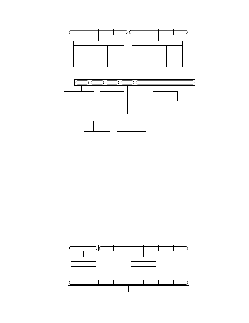
Figure 50. Teletext Control Register
CGMS CRC CHECK
CONTROL
C/W04
0
1
DISABLE
ENABLE
WIDE SCREEN SIGNAL
CONTROL
C/W07
0
1
DISABLE
ENABLE
C/W07
C/W06
C/W05
C/W04
C/W03
C/W02
C/W01
C/W00
CGMS ODD FIELD
CONTROL
C/W05
0
1
DISABLE
ENABLE
C/W03–C/W00
CGMS DATA BITS
CGMS EVEN FIELD
CONTROL
C/W06
0
1
DISABLE
ENABLE
Figure 51. CGMS_WSS Register 0
C/W0 BIT DESCRIPTION
CGMS Data Bits (C/W03–C/W00)
These four data bits are the final four bits of CGMS data output
stream. Note it is CGMS data ONLY in these bit positions, i.e.,
WSS data does not share this location.
CGMS CRC Check Control (C/W04)
When this bit is enabled (“1”), the last six bits of the CGMS
data, i.e., the CRC check sequence, is calculated internally by
the ADV7170/ADV7171. If this bit is disabled (“0”) the CRC
values in the register are output to the CGMS data stream.
CGMS Odd Field Control (C/W05)
When this bit is set (“1”), CGMS is enabled for odd fields.
Note this is only valid in NTSC mode.
CGMS Even Field Control (C/W06)
When this bit is set (“1”), CGMS is enabled for even fields.
Note this is only valid in NTSC mode.
WSS Control (C/W07)
When this bit is set (“1”), wide screen signaling is enabled. Note
this is only valid in PAL mode.
CGMS_WSS REGISTER 1 C/W1 (C/W17–C/W10)
(Address [SR4–SR0] = 17H)
CGMS_WSS register 1 is an 8-bit-wide register. Figure 52
shows the operations under the control of this register.
C/W1 BIT DESCRIPTION
CGMS/WSS Data Bits (C/W15–C/W10)
These bit locations are shared by CGMS data and WSS data. In
NTSC mode these bits are CGMS data. In PAL mode these
bits are WSS data.
CGMS Data Bits (C/W17–C/W16)
These bits are CGMS data bits only.
CGMS_WSS REGISTER 2 C/W1 (C/W27–C/W20)
(Address [SR4–SR0] = 18H)
CGMS_WSS register 2 is an 8-bit-wide register. Figure 53
shows the operations under the control of this register.
C/W2 BIT DESCRIPTION
CGMS/WSS Data Bits (C/W27–C/W20)
These bit locations are shared by CGMS data and WSS data. In
NTSC mode these bits are CGMS data. In PAL mode these
bits are WSS data.
C/W17
C/W16
C/W15
C/W14
C/W13
C/W12
C/W11
C/W10
C/W15–C/W10
CGMS/WSS DATA
C/W17 C/W16
CGMS DATA ONLY
Figure 52. CGMS_WSS Register 1
C/W27
C/W26
C/W25
C/W24
C/W23
C/W22
C/W21
C/W20
C/W27–C/W20
CGMS/WSS DATA
Figure 53. CGMS_WSS Register 2
相關PDF資料 |
PDF描述 |
|---|---|
| ADV7170SU | Digital PAL/NTSC Video Encoder with 10-Bit SSAF⑩ and Advanced Power Management |
| ADV7171KS | Digital PAL/NTSC Video Encoder with 10-Bit SSAF⑩ and Advanced Power Management |
| ADV7171SU | Digital PAL/NTSC Video Encoder with 10-Bit SSAF⑩ and Advanced Power Management |
| ADV7171* | Digital PAL/NTSC Video Encoder with 10-Bit SSAF and Advanced Power Management |
| ADV7171 | Digital PAL/NTSC Video Encoder(數字PAL/NTSC視頻編碼器) |
相關代理商/技術參數 |
參數描述 |
|---|---|
| ADV7170KSUZ | 制造商:AD 制造商全稱:Analog Devices 功能描述:Digital PAL/NTSC Video Encoder |
| ADV7170KSUZ-REEL | 制造商:AD 制造商全稱:Analog Devices 功能描述:Digital PAL/NTSC Video Encoder |
| ADV7170KSZ | 制造商:AD 制造商全稱:Analog Devices 功能描述:Digital PAL/NTSC Video Encoder |
| ADV7170KSZ-REEL | 制造商:AD 制造商全稱:Analog Devices 功能描述:Digital PAL/NTSC Video Encoder |
| ADV7170SU | 制造商:AD 制造商全稱:Analog Devices 功能描述:Digital PAL/NTSC Video Encoder with 10-Bit SSAF⑩ and Advanced Power Management |
發布緊急采購,3分鐘左右您將得到回復。